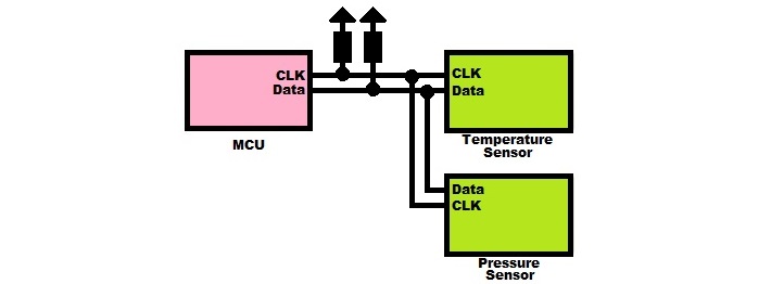
I2C is one of the three fundamental
serial communication protocols
used by CPUs (MCU, MPU, DSP,
GPU, etc) to communicate with
external-to-CPU internal-to-PCB
slave IC devices. Hardware
wise, the protocol requires requires
exactly two pins (CLK and DATA) and
two pull-up resistors. The CLK pin
is typically driven by the master
while the DATA pin is driven by
both the master and the slave devices.
With I2C, a CPU can communicate with
up to 172 devices at a time.
Advantages
Requires only two pins.
Can communicate with 172 devices.
Dissadvantages
Steep learning curve.
Considered hard to debug.
Protocol half duplex which means only device (either master or slave) can communicate at a time.
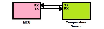
UART
Description
UART is one of the three fundamental serial communication protocols used by CPUs (MCU, MPU, DSP, GPU, etc) to communicate with external slave IC devies. Unlike other serial communication protocols, with UART there is no concept of master and slave; both the CPU and the target device are a master and a slave. Hardware wise, the protocol requires requires only two pins (TX and RX). Although the communication protocols as a whole is full-duplex, each RX/TX pair is a half-duplex line. UART is actually a legacy communication protocol which was used by desktop computers to connect mice and keyboards to the computer tower. With the help of a MAX-232 chip, the voltages could be amplified/reduced for noise suppression and external communication.
Advantages
Most mature of the serial communication protocol..
Most ubiquitous serial communication protocol
Easiest theory to understand.
Dissadvantages
Slow
Outdated
Can only communicate with one device
SPI
Description
I2C is one of the three fundamental
serial communication protocols
used by CPUs (MCU, MPU, DSP,
GPU, etc) to communicate with
external slave IC devies. Hardware
wise, the protocol requires requires
exactly two pins (CLK and DATA) and
two pull-up resistors. The CLK pin
is typically driven by the master
while the DATA pin is driven by
both the master and the slave devices.
With I2C, a CPU can communicate with
up to 172 devices at a time.
Advantages
Requires only two pins.
Can communicate with 172 devices.
Dissadvantages
Steep learning curve.
Considered hard to debug.
Protocol half duplex which means only device (either master or slave) can communicate at a time.
Micrcontroller (MCU)
Introcution
Microcontrollers (MCU) are low cost alternatives to microprocessors (MPU). Unlike MPUs, which are general purpose processors, MCUs are dedicated purpose processors which means their behavior and sense of purpose is set in stone from the factory. Furthermore, not only can an MCU run only one application at a time but it runs that same application all the time. In addition, unlike a microprocessor, MCUs integrates its CPU, primary memory (RAM) and secondary memory (Flash) into a single IC die chip. The upside to this configuration is a reduction in cost, power consumption, footprint and complexity however the caveat is it limits primary memory, secondary memory, and processing power. Whatsmore, writing “firmware” for a MCU requires intimate knowledge of the hardware environment in which the application runs. MCU programmers must know only what “periherals” their MCU (SPI, I2C, UART, DMA, ADC, DAC, TIMER, etc) has, what traces are connected to what I/O pins, memory usage, CPU frequency, etc. Finally, most MCU use the reduced instruction set computer (RISC) architecture.
Operation
Unlike in an MPU where application code is executed from primary memory, in an MCU computer system application code is executed directly from secondary memory. This presents a problem as the CPU is extremely fast (3 GHz) and secondary memory (16 MHz) is extremely slow. As a result, the CPU frequency is typically throttled to match that of secondary memory. That means the fastest an MCU can be clocked is equal to or less than the frequency of the secondary memory. Engineers have figured out ways around this bottleneck (block read, buffers, cache, etc.) however that is beyond the scope of this "pop-up".
In the MCU world, application code is better known as firmware. Firmware consist of instructions and variables. Secondary memory is used for firmware instructions while primary memory is used for firmware variables. Furthermore, in the MCU world, there is no need for operating system. MCU secondary memory is so small that only one application fits. In addition, because MCU CPU frequency throttled so much, only one single application can reasonably be execute at a time.
Lingo
MCU – Short for microcontrolller, is the all-in-one computer system which houses not only the CPU, primary memory (RAM) and secondary memory (HDD, SSD, Flash, FRAM, etc.) in a single IC die chip, but also the firmware which controls the MCU. See “Introduction” above.
Firmware - This is the program which loaded into the MCU and which controls its behavior. More often than not, the firmware is created in an integrated development environment (IDE), cross-compiled from a CISC environment to a RISC instruction set, and finally is loaded into the MCU secondary memory (which is typically Flash). Unlike OS applications which make system calls, firmware is created to specifically talk to the hardware (reading/writing from/to registers).
Peripherals - a.k.a. hardware modules and hardware accelerators are tiny independent micro-circuits embedded in a MCU die that either give the MCU extra capabilities (ADC, DAC) or offload mundane tasks from the CPU (UART, SPI, I2C, PWM). Peripherals not only reduces MCU power consumption but also allows the much more efficient use of the CPU by offloading mundane repetitive tasks to the low power peripherals. Each peripheral is configured via a set of registers. Furthermore, there are a variety of peripherals each with a specific purpose.
I2C - One of the three fundamental serial communication protocols used by CPUs to communicate with external slave IC devies. Hardware wise, the protocol requires requires exactly two pins (CLK and DATA) and two pull-up resistors.
SPI - One of the three fundamental serial communication protocols used by CPUs to communicate with external slave IC devies. Hardware wise, the protocol requires requires exactly four pins (MISO, MOSI, CL, CS).
UART - One of the three fundamental serial communication protocols used by CPUs to communicate with external slave IC devies. Hardware wise, the protocol requires requires exactly two pins (TX and RX).
ADC - Mixed signal peripheral which takes analog signals generated by analog sensors (temperature, pressure, humidity, PPG ECG, etc) and converts them into digital signals which the MCU can understand.
ADC - Mixed signal peripheral which takes digital signals generated by the MCU and converts them into one continuous analog signal. A typical application would be to drive speaker/driver.
PWM - Generates a digital square wave with different frequency and duty cycle.
DMA - Transfers incoming/outgoing data generated by other peripherals (I2C, SPI, UART, ADC, DAC, etc) to/from MCU data memory, respectively, with little to no CPU intervention.
Registers - Special memory address that are used to control the behavior of MCU “peripherals”. Writing to these memory address has a direct impact on the peripherals behavior (enables, disables, speed, Interrupt, etc). Each and every peripheral has a range of address which configure its behavior.
Integrated Development Environment (IDE) – The “host side” computer application that is used to construct the “target side” MCU firmware. An IDE consist of a text editor, cross-compiler and a debugger.
Unlike their MCU counterparts which are dedicated purpose processors, a microprocessor is a general purpose processor which means that the computer system’s behavior and sense of purpose is not set in stone but instead dictated by which application is currently executing. Unlike an MCU, a MPU can select from a list of applications to run and it can run them concurrently. Furthermore, unlike MCU counterparts, both the primary memory (RAM) and secondary memory (Flash, HHD, SSD, etc) are completely scalable. This is due to the CPU, primary memory and secondary memory being housed in separate ICs. Primary memory and secondary memory can be increases simply by replacing the respective IC. Whatsmore, because microprocessors are too complex and powerful to be run by any single application, typically they are managed by an operating system. As a result, MPU applications don’t directly run on a microprocessor but instead make system calls to the OS whenever a hardware resource is needed. Finally, MPUs use both reduced instruction set computer (RISC) and Complex Instruction Set Computer (CISC).
Operation
There are three types of memory found on a MPU based computer system; primary memory, secondary memory and EEPROM. Each not only has its advantages and disadvantages, but also its purpose. Primary memory is volatile, which means its contents is forgotten when the power is turned off. Furthermore, primary memory has a fast access speed however its storage capacity is small. Conversely, secondary memory is non-volatile, slow and it storage capacity is large. EEPROM is the worser of all three types of memories; not only does EEPROM have a smaller storage capacity compared to primary memory but also has a slower access speed than secondary memory. EEPROM, however, has the most important task during MPU startup.
When the MPU computer system is initially powered on, primary memory, being volatile, is empty. This presents a problem as the CPU mainly executes instructions from primary memory and both the operating system and the computer applications reside in the secondary memory. Turns out the CPU can also execute instructions from EEPROM. EEPROM is non-volatile like secondary memory and it houses one simple yet extremely important application; the Boot loader. The Boot loader is a small programs that executes only during power up and whose one and only job is to copy the operating system from secondary memory to primary memory. Once the transfer is complete, the boot loader hands off control to the primary memory/operating system. Once the operating system is in control it takes care of copying the application from the secondary memory to the primary memory whenever a user launches an application.
Lingo
MPU – Short for microprocessor, is the central processing unit (CPU) in a computer system. Unlike a MCU which is a non scalable all-in-one computer system, a MPU modulates its primary memory (RAM) and secondary memory (Flash, HDD, SSD, FRAM, etc). With a MPU based computer system, memory increase is as simple as chip replacement.
Primary Memory (PM) - PM Is sandwiched between CPU and secondary memory (SM). PM is typically either SRAM or DRAM technology. PM has the advantage that it has fast access speed (both read and write). The disadvantage is that PM tends to be expense and hence only small quantities is present. Furthermore, PM tends to be volatile which means its contents is forgotten power is removed. In a MPU architecture, the CPU fetches and executes instructions from PM only.
Secondary Memory (PM) - SM is physically connected only to primary memory (and DMA). It is typically made up of either HDD, SSD, FLASH, etc. It is slow compared to PM and much slower compared to CPU frequency however what is lacks in speed it makes up for in storage capacity. SM has a storage capacity that is millions if not billions of times larger than PM. In addition, SM is volatile which means it does not forget it contents when power is removed.
Applications/Operating Systems - Microprocessors are way too complex and powerful to execute any one single application. Instead, microprocessors not only execute one application from a list of applications but do so concurrency. Furthermore, due to the power and complexity of MPUs, its resources (memory, peripherals, I/O, etc) are manged by an operating system instead of directly by an application. Unlike MCUs which directly interact with the hardware whenever a resource is needed, MPU applications make system calls to the OS whenever they require a hardware resource.
Windows/Windows ES
Linux/Embedded Linux
Android
Integrated Development Environment (IDE) - The IDE is the “host side” computer application that is used to construct the “target side” MPU application. An IDE consist of a text editor, compiler and a debugger. Cross compilation occurs only if the target side architecture (CISC) is different from the host side architecture (RISC) which is typically the case when it comes to MCU.
Dissadvantages
Costlier
Larger power consumption
Larger PCB real-estate footprint
Complex PCB layout - ADDR and DATA lines
Advantages
More powerfull
Increased processing execution speed - 3 GHz
Increased processing power - 1M MIPS
General Purpose
Dynamic applications execution
Concurent application execution
Multi-program multi-application-execution
Operating system support
Windows
Linux
Android
Vendors/Name/Architecture
Intel - x86 & x64
AMD - x86 & x64
ARM - Texas Instruments & Microchip
Texas Instruments - OMAP
Timer
General-Peripheral Explanation
(a.k.a. hardware modules, hardware accelerators) are tiny autonomous micro-circuits embedded in a CPU die that give the CPU extra capabilities, reduces its power consumption and/or increase its processing efficiency. Examples of peripherals include; UART peripheral, I2C peripheral, SPI peripheral, ADC peripheral, DAC peripheral, Timer peripheral, etc. Peripherals were invented/designed for off-loadable CPU tasks (simple, mundane, repetitive, sequential and non-conditinal). Whenever possible it is better to offload a off-loadable task from the CPU to the peripherals as peripherals consume much less energy than a CPU. Constructive use of peripherals results not only reduction in embedded system power consumption but also increases CPU instruction execution throughput. Each peripheral is configured by reading/writing to special memory addresses called registers. Each peripheral is controlled by a range of memory addresses. Each memory cell or group of memory cells in a register memory location adjusts the peripherals behavior is one way or another (enable, disable, increase/decrease peripheral speed, etc).
Timer (Simplified Explanation)
Sometimes called a counter, the Timer is one of the most basic peripherals that can be found in a CPU. The most simplest Timer peripheral counts from 0 to a configured limit. Not only can the Timer clock come from any number of sources (GPIO, CPU clock, oscillator), but it can be set to any frequency and can even be aperiodic. Furthermore, typical counter limits are 28 and 216. Upon reaching that predefined limit, the timer typically generates an interrupt. That interrupt signal can be tied to any number or things/circuits however the most common scenario is that the signal is tied to the CPU.
Application Scenario (Simplified Explanation)
In a typical scenario the Timer acts as an alarm clock for the CPU. In a battery operated embedded systems, it is desired to extend the batter life as much as possible. This is accomplished by through several ways however the simplest and effective is to keep the CPU powered down as much as possible and wake it up only when needed. This is due to the fact that the CPU consumes way more power than the Timer peripheral. Most task needed to be executed by the CPU are simple and sporadic. In addition, most tasks are completed by the CPU within few microseconds. All these attributes make the Timer peripheral the ideal.
During peripheral initialization, the CPU not only enables the Timer but also configures its operation (clock source, clock frequency, count limit, etc.). After peripheral initialization and before the CPU goes officially to sleep, the Timer is started. While the timer is counting, the CPU is asleep conserving some much needed power. When the timer finishes counting, it generates an interrupt and in the process wakes up the CPU. The CPU wakes up, executes the list of tasks it must complete, resets/starts the Timer, and finally goes back to sleep.
Typical Registers
Like all CPU peripherals, the Timer peripheral is configured through a series of “registers”. Registers are special memory addresses that don’t store and should not be used to store information/data. Register memory cells are wired to peripheral input/output circuits configuration pins. The peripherals behavior can be altered simply by writing to these memory address. Similarly, the peripherals results can be obtained by reading from these memory location.
Timer Clock Source – The clock going into the Timer can come from any number of sources. Typically sources include (GPIO, CPU clock, oscillator). The most typical scenario is that the Timer clock source comes from the same source as that of the CPU clock.
Timer Clock Divider - This register divides the Timer clock. The slower the clock, the less it wakes up the CPU and the more power is conserved. Conversely, the faster the clock, the faster tasks get executed however the more power is consumed.
Timer limit - This sets the upper bound limit for the Timer counter register. The lower the limit, the more often the Timer interrupts.
Timer Counter - This registers holds the current counter value. The value increments after ever clock tick.
Enable/disable Timer - Like all other peripherals, the Timer peripheral consumes power when enabled. In instances when the Timer peripheral is not needed, it can be powered down resulting in power savings.
Start/pause/reset Timer - Sometimes it is desired to start, stop and reset the timer counter.
GPIO
Peripheral Explanation
(a.k.a. hardware modules, hardware accelerators) are tiny autonomous micro-circuits embedded in a CPU die that give the CPU extra capabilities, reduces its power consumption and/or increase its processing efficiency. Examples of peripherals include; UART peripheral, I2C peripheral, SPI peripheral, ADC peripheral, DAC peripheral, Timer peripheral, etc. Peripherals were invented/designed for off-loadable CPU tasks (simple, mundane, repetitive, sequential and non-conditinal). Whenever possible it is better to offload a off-loadable task from the CPU to the peripherals as peripherals consume much less energy than a CPU. Constructive use of peripherals results not only reduction in embedded system power consumption but also increases CPU instruction execution throughput. Each peripheral is configured by reading/writing to special memory addresses called registers. Each peripheral is controlled by a range of memory addresses. Each memory cell or group of memory cells in a register memory location adjusts the peripherals behavior is one way or another (enable, disable, increase/decrease peripheral speed, etc).
ADC
Peripheral Explanation
(a.k.a. hardware modules, hardware accelerators) are tiny autonomous micro-circuits embedded in a CPU die that give the CPU extra capabilities, reduces its power consumption and/or increase its processing efficiency. Examples of peripherals include; UART peripheral, I2C peripheral, SPI peripheral, ADC peripheral, DAC peripheral, Timer peripheral, etc. Peripherals were invented/designed for off-loadable CPU tasks (simple, mundane, repetitive, sequential and non-conditinal). Whenever possible it is better to offload a off-loadable task from the CPU to the peripherals as peripherals consume much less energy than a CPU. Constructive use of peripherals results not only reduction in embedded system power consumption but also increases CPU instruction execution throughput. Each peripheral is configured by reading/writing to special memory addresses called registers. Each peripheral is controlled by a range of memory addresses. Each memory cell or group of memory cells in a register memory location adjusts the peripherals behavior is one way or another (enable, disable, increase/decrease peripheral speed, etc).
ADC Introduction
CPUs are electronic devices that think, act, talk and behave in a “digital” manner; In fact the native language of a CPU is 0s and 1s. 0 represents 0 volts and 1 typically represents 3.3 and 5 volts. From the CPUs perspective however the world is “analog”; it can have infinite in-between (1.024, 1.24, 2.4, etc) values. Light intensity, humidity, temperature, pressure, sound, ECG, PPG, etc are all examples of analog signals that we are interested not only in measuring, but also processing and recording. Almost always the sensor circuits that are designed to detect and measure these analog signals must themselves be analog. They encoded the analog information they are measuring into an analog signal. This presents a problem as CPUs only understand in 1s and 0s (0 or 3.3 volts) whereas the analog sensor circuits output the measurement as voltages that range everywhere between 0 and 3.3 volts. This is where the analog-to-digital (ADC) converter comes in. A ADC converts the analog signal to something the CPU can understand which is 0s and 1s.
The process of converting and mapping a continuous analog signal produced by the analog sensor circuit into its digital counterpart is a deceptively simple yet misleading process. Technically wise, we say that an analog signal is a summation of sinusoids of varying frequencies each with a varying amplitude. Non-technically wise, we say that an analog signal is a continuous analog signal whose amplitude varies with time. Sometimes the analog signal’s amplitude is slow changing (temperature, pressure, etc) other times it is mid-changing (voice, ECG and PPG) while other times it is fast changing. There is a limit to how fast an analog signal can “change” and have the ADC record the change. Technically speaking, there is a limit as to how “fast” an analog signals amplitude can change and still have the ADC record that change. Standardization between the sensor circuit and the ADC dictates that voltage between them will will never exceed the agreed upon lower (typically 0) and upper (typically 3.3 volts) limit. The job of the ADC is to break up the voltage signal into discrete units each representing the voltage/amplitude at that particular point in time.
Although it is very common to find ADC circuits are available as discrete IC packages, for the rest of this discussion ADC refers to ADC circuit integrated into a CPU die and accessed as a standard peripheral. It should be emphasized that not all CPUs are equipped with a ADC peripheral. It is stated that without hesitation the ADC peripheral is by far one of the most complex peripherals found in a typical CPU. Like most peripherals, there are a variety of ways to implement an ADC each with its advantage and disadvantage. Most ADC consists of the following data signals; Vin, Vref, Vout. Vin refers to the analog voltage being converted. Vref refers to the reference voltage. Vout is converter analog signal.
Lingo
Resolution – When dealing with ADCs, resolution is one of the, if not the, most important specs when evaluating a ADC’s potential performance. To truly grasp the concept of resolution it is vital to understand the different perspectives that come together during ADC conversion; analog sensor circuit (ASC) perspective, analog signal perspective and ADC perspective. First is the ASC which generates the analog signal which is feed into the ADC. Standardization between the ASC and the ADC dictates that the analog signal generated by the ASC will never exceed the agreed upon lower and upper limits, typically 0 and 3.3 volts, respectively. The analog signal is allowed to fluctuate anywhere in-between agreed upon upper and lower limits but never exceed it. Technically speaking these voltage limits are refereed to as peak-to-peak (Vp-p). The task of the ADC upon sampling the analog must assign it a digital value. How many possible values it can assigns is dependent on the resolution and what digital value it assigns is dependent on Vin, Vref and resolution. Resolution dictates how many available digital values you can assign a sampled analog signal. Common resolution levels include 8-bit (256 values), 16-bit (65,536 values) and 24-bit (16,777,216 values). The lowest an 8-bit can assign is 0 and the highest is 255. Similarly, the lowest and highest a 16-bit and 24-bit ADC can assign is 0 and 0 and 65,535 and 16,777,215, respectively. The formula which ADC use to solve for Vout given Vin, Vref and resolution variables is given by...The greater the resolution the more accurate you can recreate the original signal. The caveat of a ADC with great resolution is it requires more memory and processing power to store and process the converted data.
Sampling Rate - The rate at which the ADC samples the analog signal is refereed, not surprisingly, to as sampling rate/frequency. When dealing with ADC’s, sampling frequency is one of the if not the most important specs when evaluating a ADC potential performance. The sampling frequency is dictated by application and capability. As mentioned in the resolution section, an analog signal is a continuous signal whose voltage amplitude varies with time. Depending on the sensor circuit, the analog signal’s amplitude can be slow changing (temperature, pressure, etc.), mid-changing (voice, ECG and PPG) or even fast changing. The rate at which the ADC should sample the incoming analog signal is dependent on the rate at which the signal changes. For instance, it does not makes sense, to sample a temperature sensor at GHz range. Conversely, it does not make sense to sample image pixel light intensities at the Hz range. As was mentioned previously, we say that an analog signal is a summation of sinusoids of varying frequencies each with a varying amplitude. The Nyquist sampling theorem states that a faithful reproduction of the original signal is only possible if the sampling rate is higher than twice the highest frequency of the signal. Therefore, when selecting the appropriate ADC for the application, it must be assured that the ADC can handle the sampling rate which is required for the application.
Quantization Error - In the process of mapping an analog voltage signal into the digital domain both rounding and truncating is unavoidable phenomena. Increasing both the sampling frequency and resolution can minimize the “quantization error” however it will always be present. Subtraction of the original analog waveform with the “quantized” one equals the “quantization noise” In a typical DSP application, the amount of noise is usually negligible when compared to other outside noise.
Aliasing – It is the authors opinion that aliasing is a phenomena that can best be described pictorially. Aliasing occurs whenever the sampling frequency is below the recommended Nyquist Sampling Rate (not recommended). As was mentioned previously, an analog signal is a summation of sinusoids of varying frequencies each with a varying amplitude. For the sake of simplicity, if we take the analog signal, break it up into its separate frequencies, feed the highest frequency sinusoid to the ADC and configure the ADC to sample that sinusoid at half the frequency, we get a totality new sinusoid. This new sinusoid is an alias of the sampled sinusoid.
ADC Architectures
Like most things in life, there isn’t a one size fits all ADC architecture. Instead there are a variety of ADC architectures which can implement a ADC. Each architecture has its advantages and disadvantages. There are a variety of architectures to choose from (direct-conversion, successive approximation, ramp-compare, Integrating, Delta-Encoded, Pipelined, Sigma-Delta, Time-Interleaved, Intermediate FM stage, etc). Typical, it is a trade off is between sampling rate, power consumption and resolution. Although CPUs typically integrate two types of ADC architectures (SAR and Sigma-Delta), it is worth mentioning/discussing other popular architectures.
Flash/Parallel ADC
Flash ADC is the simplest, fastest and easiest to comprehend of all the ADC architectures currently available. Architecturally wise a Flash ADC type only consists of; a parallel bank of high speed comparators, an error correction circuity and an encoder. Unlike other ADC arhitecutre types which which “narrow-in” on a ADC conversion-result over “a series of stages”, Flash ADC obtains the conversion result in a single parallel step. Conversion time is limited only by the speed of the comparators and priority encoder. Typical applications include; radar detection, wideband radio receivers, oscilloscopes, and optical communication links. Furthermore, Flash ADC is the most expensive ADC architecture as well. Comparators, as it turns out, are expensive, large, and power hungry. This presents a problem as Flash converters requires comparators and a lot number of them. This problem is exacerbated as resolution of the ADC is directly related to a the number of comparators. A N-bit resolution Flash ADC requires 2N-1 comparators and 2N high precision laser trimmed resistors. This makes Flash converters impractical for precision's much greater than 8-bits as the size, power consumption and cost of all those comparators would exceed practical limitations.
Resolution
Comparators
Laser Trimmed Resistors
2
3
4
3
7
8
4
15
16
5
31
32
6
60
64
7
127
128
8
255
256
Parallel Comparator Bank – The parallel bank comparators servers as the input to the Flash ADC. As can be seen, the sampled analog signal Vin signal is directly connected to every comparator non-inverting input pin. Conversely, Vref is indirectly connected, through a “resistor ladder” circuit, to every comparator inverting input pin. Each comparator generates a logical 0 or 1 depending on whether the Vin analog voltage is greater or less than the voltage divider reading from the resistor ladder.
Resistor ladder – The resister ladder is nothing but a series of resistors which are voltage divided and are meant to break up the Vref signal to equal sized voltages. The resistors which are used to construct the resistor ladder are high precision laser trimmed.
Bubble Error Correction – Sometimes, the environment in which the Flash ADC is exposed to is so harsh that comparator premature failure results. In those rare instances, the comparator output gets stuck either high or low. The Bubble error correction is a digital redundancy correction mechanism that both detects and “repairs” any comparators with faulty output issues.
Priority Encoder – Sometimes, the environment in which the Flash ADC is placed is so harsh that comparator premature failure occurs. The typical scenario is that a faulty comparator output will be stuck either high or low. The Bubble error correction is a digital redundancy correction mechanism that “repairs” any comparators with a stuck output pin.
Advantages
ADC theory simple to grasp
Fast sampling rate (gigahertz)
Dissadvantages
8 bits of resolution or fewer
Lower power consumption
Non-scalable
Comparator number doubles for each added bit.
ADC - SAR
ADC Introduction
The SAR ADC is the most common type of ADC architecture due to their low cost, low power consumption, generally accuracy, fast and have a small form factor. Both their sampling frequencies and resolution are soo average, that they are ideal for general purpose applications. The main subcircuit building blocks for a SAR ADC type include; a sample-and-hold circuit, a comparator, successive-approximation register (SAR), digital-to-analog converter, and control logic. A result is produced an n-bit output in n clock cycles of its clock. Sampling times vary from less than 1 microsecond to 50 microsecond (2-5 Msps). Typical resolution for the type of ADCs is between 8-bits and 16-bits.
Unlike in a Flash ADC, in a SAR ADC, the process of converting the analog signal into its digital counterpart is an iterative process. With each successive loop the ADC is converging down to its on the digital counterpart. Mathematically speaking, it is said that the SAR ADC implement a binary search algorithm. With each pass, the DAC outputs a voltage that is either 1.5 as big and the prior voltage or 0.5 of the prior voltage. As can be seen, with every loop the DAC output is not only a different voltage but a ratio of Vref. The number of passes is directly proportional to the resolution of the ADC.
Comparator – The comparator compares the analog input signal Vin to DAC voltage. Although after each iteration the non-inverting input analog signal stays the same, the inverting DAC signal always changes. Initially, the DAC voltage is set to Vref/2. Subsequent iterations set the DAC to output a voltage to be either 1.5 the privouse iteration or 0.5 of the previous iteration. This process repeats itself until all the bits in the SAR register are analyzed.
Control Logic – Among other things, the control logic calculates what new value that should be stored in the SAR register. It makes this calculation based on previous value stored in the SAR register and on the result from the comparator comparison. The control logic analyses and configures the value stored in the SAR register from left to right. During the first iteration, for example, the control logic sets the left most bit in the SAR register. During the second iteration it either clears (Vin less than DAC) or leaves set (Vin greater than DAC) the previous analyzed bit, however it always sets the next bit. This process repeats itself until all the bits in the SAR register are analyzed.
SAR – The output from the SAR register is used as input to the DAC. The SAR register dictates to the DAC what voltage is should be outputting for the current iteration. Just like like a CPU register, the SAR register is a memory circuit which data. More specifically, the SAR register saves/holds the current/previous binary iteration value. The contents of the SAR register in the following iteration will be either 0.5 or 1.5 the previous iteration content value.
DAC – Like ADC there are a variety of architectures to choose from when implement a DAC in a SAR ADC. Many SAR ADCs use a capacitive DACs that provides an inherent track/hold function. Which each loop, the DAC should output a different voltage which is dictated by the SAR register.
Advantages
Low Cost
Low power
Decenlyt Fast
Small form factor
Dissadvantages
Slow to respond to sudden jumps in the input signal
Vin spikes can be disastrous
Single-Slope ADC
Dual-Slope ADC
DAC
Peripheral Explanation
(a.k.a. hardware modules, hardware accelerators) are tiny autonomous micro-circuits embedded in a CPU die that give the CPU extra capabilities, reduces its power consumption and/or increase its processing efficiency. Examples of peripherals include; UART peripheral, I2C peripheral, SPI peripheral, ADC peripheral, DAC peripheral, Timer peripheral, etc. Peripherals were invented/designed for off-loadable CPU tasks (simple, mundane, repetitive, sequential and non-conditinal). Whenever possible it is better to offload a off-loadable task from the CPU to the peripherals as peripherals consume much less energy than a CPU. Constructive use of peripherals results not only reduction in embedded system power consumption but also increases CPU instruction execution throughput. Each peripheral is configured by reading/writing to special memory addresses called registers. Each peripheral is controlled by a range of memory addresses. Each memory cell or group of memory cells in a register memory location adjusts the peripherals behavior is one way or another (enable, disable, increase/decrease peripheral speed, etc).
Pulse Width Modulation
Peripheral Explanation
(a.k.a. hardware modules, hardware accelerators) are tiny autonomous micro-circuits embedded in a CPU die that give the CPU extra capabilities, reduces its power consumption and/or increase its processing efficiency. Examples of peripherals include; UART peripheral, I2C peripheral, SPI peripheral, ADC peripheral, DAC peripheral, Timer peripheral, etc. Peripherals were invented/designed for off-loadable CPU tasks (simple, mundane, repetitive, sequential and non-conditinal). Whenever possible it is better to offload a off-loadable task from the CPU to the peripherals as peripherals consume much less energy than a CPU. Constructive use of peripherals results not only reduction in embedded system power consumption but also increases CPU instruction execution throughput. Each peripheral is configured by reading/writing to special memory addresses called registers. Each peripheral is controlled by a range of memory addresses. Each memory cell or group of memory cells in a register memory location adjusts the peripherals behavior is one way or another (enable, disable, increase/decrease peripheral speed, etc).
PWM Introduction
Electric motors and incandescent lights have been around for more that a millennium. For the most part the technology was solid - dependable, reliable and affordable. However a problem arose whenever the full output power was not desired. At that time, either you were provide the entire power (on) or it provided no power at all (off). The problem arose whenever you wanted say 25%, 50% or 75% power. Take for instance an electric motor where you would want it to rotate at half the speed or a light bulb that you wanted in at half brightness. There was a solution however the solution was by no means solid – it was big, bulky, unreliable and wasteful. Prior to PWM, the only way to “control” electrical power was through power dissipation; a potentiometer or rheostat, was placed in series with the load and the excess power was dissipated as heat. PWM is a method whereby a “PWM signal” is generated by a “PWM circuit” for the purposes of efficiently powering a load. The average value of voltage (and current) fed to the load is controlled by effectively chopping up the power into discrete bursts. With time, it was realized that PWM had more applications that electric motors and lightbulbs. Today the loads vary from signal based (LED and Servo Motor) to power based (Stove Heating Element, speaker/driver to Permanent-Magnet Direct-Current motor). A PWM signal resembles a square wave however they do have their differences. Whats-more, there are a variety of PWM circuits which can generate PWM signals.
PWM Architectures
There are a variety of “ways” to generate a PWM signal. In actuality when we say “ways”, what we really mean are architectures. Not one PWM architecture is “better” than the other, moreof each offers something that the other does not. The PWM circuit implemented by most CPUs and the one we will be discussing here is the time-proportioning (TP) based PWM circuit. Although, TP based PWM circuits are available as discrete IC packages, for the rest of this discussion when we say PWM we refer to TP based PWM circuit integrated into a CPU die and accessed as a standard peripheral. In fact, in a CPU a TP based PWM is implemented with the use of a regular Timer counter circuit.
Intersective Method
Delta
Delta-sigma
Space vector modulation
Direct torque control (DTC)
Time proportioning
And like the RTC and WDT peripherals, TP based PWM peripheral can also serve as an emergency Timer. A TP based PWM peripheral generates a PWM signal with little to no CPU intervention other than initial register configuration. This permits the CPU to either be powered down or busy completing another tasks. In a TP based PWM circuit, the counter limit is used as the PWM period. The smaller the counter limit is set, the smaller the PWM period and vice versa. Furthermore, the overflow interrupt is used to reset the PWM signal. The timer compare interrupt is used to configure the PWM duty cycle. The smaller the PWM compare interrupt, the smaller the PWM signal duty cycle and vice versa.
PWM vs Square Wave
The PWM signals resemble a square waves; they look and acts much like them. In fact a PWM signal with exactly 50% “duty cycle” and a Ymin equal to 0 is a square wave. Duty cycle is the percentage of time the amplitude is one value over the signal period times 100. Furthermore, Like a square wave, the amplitude of a PWM signals is binary; its either one value or another. Whatsmore, like a square wave, a PWM signal can have any frequency/period. Unlike a square wave, a PWM signal can have a “duty cycle” other than 50% (e.g. 0%, 25%, 75%, and even 100%). Furthermore, a PWM signal can only have lower bound amplitude of zero. Finally, in a PWM signal neither the frequency nor the duty cycle are fixed; both can and usually do change from period to period.
Typical PWM loads/applications
Although PWM theory can be used to transfer data, it is almost always used to transfer power. In this scenario, a PWM circuit/signal can be though of as a variable power supply. PWE reduces the average electrical power delivered to a load, by effectively chopping power signal up into discrete electrical power pulses. The power transfer is directly correlated to PWM signal frequency and its duty cycle. PWM exploits the fact that some loads are “slow to react” and hence don’t need constant power. PWM can be used to effectively drive a variety of loads from the small (LED brightness and servo motor shaft angle), to the medium (Permanent-magnet direct-current motor angular speed) to heavy duty (heating elements used in electric stoves, boilers, and furnace).
Stove heating element -
LED (brightness)
Servo motor (shaft angle)
Permanent-magnet direct-current motor (angular speed)
Take for instance electrics motors. When power is “removed” from an electric motor, the rotor does not immediately stop spinning, instead continues to spin for quite some time. This is directly related to Newton’s first law of motion which states object in motion will stay in motion unless acted on by an external force. According to this law the motor should want to continue to spin indefinitely. After the motor starts spinning, all it takes is a nudge to keep it spinning. With PWM, those small pulses of electrical energy is all that is needed to keep the shaft of the electric motor rotating.
Another example would be an electric stove. Ask any cook and they will confirm that it takes time for a stove/food top to heat up/cool down when enabled/disabled, respectively. When the stove is initially turned on, the temperature increase is gradual. Similarly when the stove is turned off, it takes a while for the stove/food to cool down. PWM exploits the fact stove top temperature is “slow to react” to control the average temperature. The stove knob controls the duty cycle for the heating element for the stove top which is approximately two cycles per minute.
Typical Registers
Like all CPU peripherals, the PWM peripheral is configured through a series of “registers”. Registers are special memory addresses that don’t store and should not be used to store information/data. Register memory cells are wired to peripheral input/output circuits configuration pins. The peripherals behavior can be altered simply by writing to these memory address. Similarly, the peripherals results can be obtained by reading from these memory location.
PWM Disable - This register-cell bit disables the PWM peripheral. It is wise idea to disable the PWM peripheral when not needed as doing so not only reduces power consumption but also allows the pin to be used by the GPIO or another peripheral.
PWM Enable – This register-cell enables the PWM peripheral. When enabled, the pin ceases to be a GPIO pin and now serves as the PWM pin for the PWM peripheral. Judicious enabling/disabling of the PWM peripheral not only reduces CPU power consumption but also increase the capabilities.
PWM Pause – This register-cell pauses the PWM peripheral. Pause is different from disable/enable in that the peripheral is partially on. Sometimes pausing a peripheral is a wiser choice than disabling due to long peripheral “power-up” time. Frequency use is a decisive factor in either disabling or pausing a peripheral.
PWM Clock Source – The clock signal going into the PWM peripheral can come from any number of sources. Typically sources include but not limited to (GPIO, CPU clock, oscillator). The most common scenario is that the PWM clock source is a scaled down version of the CPU clock source.
PWM Clock Divider - Typically PWM peripherals are equipped with a clock divider. A PWM clock divider provides further refinement to the PWM clock. In many instances, the source clock is too fast for the PWM peripheral.
PWM Compare Interrupt - This sets the upper bound limit for the Timer counter register. The lower the limit, the more often the Timer interrupts.
PWM Counter - This register contains the current PWM counter value. Once the value is equals the value set in the PWM Limit register, a PWM overflow occurs and the Overflow Interrupt is generated.
Watchdog Timer
Peripheral Explanation
(a.k.a. hardware modules, hardware accelerators) are tiny autonomous micro-circuits embedded in a CPU die that give the CPU extra capabilities, reduces its power consumption and/or increase its processing efficiency. Examples of peripherals include; UART peripheral, I2C peripheral, SPI peripheral, ADC peripheral, DAC peripheral, Timer peripheral, etc. Peripherals were invented/designed for off-loadable CPU tasks (simple, mundane, repetitive, sequential and non-conditinal). Whenever possible it is better to offload a off-loadable task from the CPU to the peripherals as peripherals consume much less energy than a CPU. Constructive use of peripherals results not only reduction in embedded system power consumption but also increases CPU instruction execution throughput. Each peripheral is configured by reading/writing to special memory addresses called registers. Each peripheral is controlled by a range of memory addresses. Each memory cell or group of memory cells in a register memory location adjusts the peripherals behavior is one way or another (enable, disable, increase/decrease peripheral speed, etc).
WDT Introduction
Watch Dog Timer is another peripheral that makes use of a Timer/Counter circuit. In instances where the WDT is not needed and an extra Timer is needed, the WDT can also double down as an extra Timer/counter. The output of the WDT circuit is directly connected to the CPU reset pin. Whenever the WDT counter register overflows, the WDT micro-circuits resets the CPU. To avoid resetting the CPU, the WDT counter should be periodically be reset; a process known as kicking the dog. When eneabled, WDT reset commands are sprinkled throughout the firmware to avoid resetting the CPU. The WDT should be used in situations where the firmware could hang such when reading from WiFi, BLE or NFC wireless transceiver where the target device could fall out of range in the middle of a read.
Typical Registers
Like all CPU peripherals, the WDG peripheral is configured through a series of “registers”. Registers are special memory addresses that don’t store and should not be used to store information/data. Register memory cells are wired to peripheral input/output circuits configuration pins. The peripherals behavior can be altered simply by writing to these memory address. Similarly, the peripherals results can be obtained by reading from these memory location.
WDT Clock Source – Like all micro-circuits that have a timer/counters, the WDT needs a clock source. The WDT clock source can come from any number of sources. Typically sources include (GPIO, CPU clock, oscillator). The most typical scenario is that the WDT clock source comes from the same source as that of the CPU clock.
WDT Clock Divider - This register divides the WDR clock. The slower the clock, the less often the dog must be kicked. Conversely, the faster the clock, the more often the dog must be kicked.
WDT Limit - This register configures the upper bounds for the WDT counter. The lower the value, the more often the dog must be kicked. Conversely, the higher the value, the less often the dog must be kicked.
WDT Counter - This register contains the current WDT counter value. Once the value is equal to the WDT Limit register, a WDT overflow Interrupt is generated and in the process the CPU is reset. Every time the dog is kicked, this register value gets reset back to zeo. Ideally, the counter value should never reach the WDT Limit.
WDT Enable - Enables the WDT.
WDT Disable - Disables the WDT. It is not always desirable to enable the WDT. It is often a good idea to power-down the WDT when not needed to conserve power. Furthermore, the WDT should be powered-down to avoid accidental CPU reset.
Comparator
Peripheral Explanation
(a.k.a. hardware modules, hardware accelerators) are tiny autonomous micro-circuits embedded in a CPU die that give the CPU extra capabilities, reduces its power consumption and/or increase its processing efficiency. Examples of peripherals include; UART peripheral, I2C peripheral, SPI peripheral, ADC peripheral, DAC peripheral, Timer peripheral, etc. Peripherals were invented/designed for off-loadable CPU tasks (simple, mundane, repetitive, sequential and non-conditinal). Whenever possible it is better to offload a off-loadable task from the CPU to the peripherals as peripherals consume much less energy than a CPU. Constructive use of peripherals results not only reduction in embedded system power consumption but also increases CPU instruction execution throughput. Each peripheral is configured by reading/writing to special memory addresses called registers. Each peripheral is controlled by a range of memory addresses. Each memory cell or group of memory cells in a register memory location adjusts the peripherals behavior is one way or another (enable, disable, increase/decrease peripheral speed, etc).
Introduction - One of the most simplest and basic peripherals that can be found in a CPU die is the Comparator peripheral. Like its discrete counterpart, a comparators inputs are analog (non-inverting V+ and inverting V-) but the output is digital. Furthermore, the comparator compares the two voltages and determines which of the two input signals is the highest. Typically, one of the voltages is variable and is the one being measured while the other is kept (Vref) static. Although at its core, an on-chip comparator is technically equal to its discrete counterpart, peripheral based comparators do have their differences. For instances peripheral based comparator are fabricated out of CMOS semiconductor technology whereas discrete comparators are constructed out of BJT semiconductor. This presents a problem as when analog signals are applied to digital CMOS gates, parasitic current can flow from VCC to GND. This parasitic current occurs if the input voltage is near the transition level of the gate.
Power Consumption - For starter it has always been know that judicious use of peripherals not only result in more efficient processing but also reduced power consumption. Unlike discrete counterparts, with an on-chip comparator you can alter the peripherals behavior, through software, with a simple flip of a register bit. For instance powering up/down the comparator, is achieve with a simple flip of a register bit. This helps in the never ending quest to reach zero power consumption. This helps conserve power by enabling the comparator only when needed and disabling when not needed.
Channels - Furthermore, typically most CPU dies contain a handful of comparators however many times the embedded system PCB is equipped with several circuits (null detectors, zero-crossing detectors, relaxation oscillator, level shifter, window detectors, absolute value detectors, etc) which are in need of a comparator. To resolve this dilemma many times peripheral comparators contain analog multiplexers at their input pins. This enables the comparators to be shared between several circuits.
Interrupt - The fact that the output of a comparator is digital and that the comparator transitions states (high-to-low or low-to-high) when the monitoring even has been detected (monitoring analog signal greater or less than Vref), makes it the ideal peripheral interrupt generator. Not only can and does a comparator “naturally” monitor an analog signal, but it “naturally” generate an CPU “interrupt-signal” when the event does occur. Unlike other peripherals which require glue logic to generate an interrupt from an event, a comparator generates an “interrupt-signal” as a default behavior. In conclusion having a comparator makes sense as you can naturally monitor an analog signal but so reduce power consumption in the process.
OpAmp
Peripheral Explanation
Peripherals (a.k.a. hardware modules, hardware accelerators) are tiny independent micro-circuits embedded in a CPU die that give the CPU extra capabilities, reduces its power consumption and/or increase its processing efficiency. Examples of peripherals include; UART peripheral, I2C peripheral, SPI peripheral, ADC peripheral, DAC peripheral, Timer peripheral, etc. Peripherals were invented/designed for off-loadable CPU tasks (simple, mundane, repetitive, sequential and ______). Whenever possible it is better to offload a off-loadable task from the CPU to the peripherals as peripherals consume much less energy than a CPU. Constructive use of peripherals results not only reduction in embedded system power consumption but also increases CPU instruction execution throughput. Each peripheral is configured by reading/writing to special memory addresses called registers. Each peripheral is controlled by a range of memory addresses. Each memory cell or group of memory cells in a register memory location adjusts the peripherals behavior is one way or another (enable, disable, increase/decrease peripheral speed, etc).
Real-Time Clock (RTC)
General-Peripheral Explanation
(a.k.a. hardware modules, hardware accelerators) are tiny autonomous micro-circuits embedded in a CPU die that give the CPU extra capabilities, reduces its power consumption and/or increase its processing efficiency. Examples of peripherals include; UART peripheral, I2C peripheral, SPI peripheral, ADC peripheral, DAC peripheral, Timer peripheral, etc. Peripherals were invented/designed for off-loadable CPU tasks (simple, mundane, repetitive, sequential and non-conditinal). Whenever possible it is better to offload a off-loadable task from the CPU to the peripherals as peripherals consume much less energy than a CPU. Constructive use of peripherals results not only reduction in embedded system power consumption but also increases CPU instruction execution throughput. Each peripheral is configured by reading/writing to special memory addresses called registers. Each peripheral is controlled by a range of memory addresses. Each memory cell or group of memory cells in a register memory location adjusts the peripherals behavior is one way or another (enable, disable, increase/decrease peripheral speed, etc).
RTC (Simplified Explanation)
Real-time Clock is another peripheral that makes use of a Timer/Counter circuit. In instances where the RTC is not needed and an extra Timer is needed, the RTC can also double down as an extra Timer/counter. Sometimes, an embedded system must keep track of current time. This can be accomplished through several means however the cheapest of most cost effective would be through the use of a real-time clock circuit. Although RTC circuits are available as discrete IC packages, for the rest of this discussion RTC refers to RTC circuit integrated into a CPU die and accessed as a standard peripheral. It should be emphasized that not all CPUs are equipped with a RTC peripheral.
RTC (Technical Explanation)
RTC peripheral is a specialized timer peripheral that calculates and keeps track of the time with little to no CPU intervention other than initial register configuration. This permits the CPU to either be powered down or busy completing another tasks. RTC circuits are so similar to Timer circuits that sometimes RTCs can serve as an additional Timer. At is core, a RTC circuit is a counter circuit.
Unlike Timers (and other peripherals as well) RTCs often have an alternate constant power sources. Alternate in that it is separate from the CPU power source and constant in that it should always be providing power. Should the power source ever stop, the RTC clock time will not only be incorrect, but must be reconfigured. Typically the alternate power sources are lithium battery or supercapacitors. Furthermore unlike other peripherals RTC has its own separate crystal oscillator circuit with 32,768 Hz piezoelectric resonator tuning fork crystal. Using such a low tuning fork crystal saves power, while remaining just above human audible frequency (20 to 20,000 Hz).
Typical Registers
Like all CPU peripherals, the RTC peripheral is configured through a series of “registers”. Registers are special memory addresses that don’t store and should not be used to store information/data. Register memory cells are wired to peripheral input/output circuits configuration pins. The peripherals behavior can be altered simply by writing to these memory address. Similarly, the peripherals results can be obtained by reading from these memory location.
RTC Counter Register – The RTC counter register contains the number of seconds that has elapsed since Unix Epox Time (January 1, 1970). An algorithm is used to convert the seconds in the CR register into an current time/date.
12/24 Register - This register determines whether the RTC provides a 12 hour or 24 hour time.
Alarm - Most RTC contains some type of RTC Alarm functionality. When enabled, an interrupt is generated whenever a particularly time/date event occurs.
Power Down - Disables the RTC.
Power-up - Enables the RTC.
Direct Memory Access
Peripheral Explanation
Peripherals (a.k.a. hardware modules, hardware accelerators) are tiny independent micro-circuits embedded in a CPU die that give the CPU extra capabilities, reduces its power consumption and/or increase its processing efficiency. Examples of peripherals include; UART peripheral, I2C peripheral, SPI peripheral, ADC peripheral, DAC peripheral, Timer peripheral, etc. Peripherals were invented/designed for off-loadable CPU tasks (simple, mundane, repetitive, sequential and ______). Whenever possible it is better to offload a off-loadable task from the CPU to the peripherals as peripherals consume much less energy than a CPU. Constructive use of peripherals results not only reduction in embedded system power consumption but also increases CPU instruction execution throughput. Each peripheral is configured by reading/writing to special memory addresses called registers. Each peripheral is controlled by a range of memory addresses. Each memory cell or group of memory cells in a register memory location adjusts the peripherals behavior is one way or another (enable, disable, increase/decrease peripheral speed, etc).
Liquid Crystal Display
Peripheral Explanation
(a.k.a. hardware modules, hardware accelerators) are tiny autonomous micro-circuits embedded in a CPU die that give the CPU extra capabilities, reduces its power consumption and/or increase its processing efficiency. Examples of peripherals include; UART peripheral, I2C peripheral, SPI peripheral, ADC peripheral, DAC peripheral, Timer peripheral, etc. Peripherals were invented/designed for off-loadable CPU tasks (simple, mundane, repetitive, sequential and non-conditinal). Whenever possible it is better to offload a off-loadable task from the CPU to the peripherals as peripherals consume much less energy than a CPU. Constructive use of peripherals results not only reduction in embedded system power consumption but also increases CPU instruction execution throughput. Each peripheral is configured by reading/writing to special memory addresses called registers. Each peripheral is controlled by a range of memory addresses. Each memory cell or group of memory cells in a register memory location adjusts the peripherals behavior is one way or another (enable, disable, increase/decrease peripheral speed, etc).
Introduction - Most if not all embedded systems must inform the user of their current status in some way or another. There are several options when it comes to informing the user of the embedded system PCB status. Not one technology that is better than the other, rather each has its advantages and disadvantages, and they each have their place in the embedded system world. Even though they inform the user of the current status, they work under an entirely different principle. Typically it is a trade-off between power consumption, cost, ease of implementation, and functionality. The current available technologies are; LED, light emitting and light absorbing displays. LEDs are the most simplest, lowest power and easiest to implement however they provide the least amount of information. Light emitting, on other hand, although works even under the cover of darkness, has the highest power consumption. Light absorbing displays are midway between LED and light emitting displays; they are low powered and provide decent amount of information. The one will will be concentrating on is the light absorbing as it provides the most information at the lowest price.
Theory of operation - Physics
LADs are passive electrical components that use light absorption to display information to the user. First we will discuss what happens inside of a LAD when nothing is being shown and then we will discuss what happens when a character is being shown.
Electromagnetic Wave – Since LADs work on the principle of light absorption, they require some sort external light source (sun, incandescent lights, CFL, etc) to function. The raw light that enters the LAD is both incoherent and “unpolarized” as it consists of a random equal mixture of em waves each having different frequencies, phases, and polarization states.
Vertical Slit Polarizer - When the raw unpolarized light waves enters the LADs the first thing the electromagnetic wave encounters is the vertical wire-grid linear polariser. A “polarizer” is an absortion filter that lets light waves of a specific polarization pass through while blocking light waves of other polarizations. Unwanted non-vertical light waves are filtered by way of absorption.
Vertically Polarized Wave - The output of (2) is a beam of well-defined single linear polarized light waves. Because the slits in (3) are oriented vertically, the raw light is polarized vertically.
Liquid Crystal – The liquid crystal is a device that has the potential to rotate the polarized light waves that travel through it. More specifically, the crystal rotates a polarized light waves by 90 degrees when no voltage is applied to it. Conversely, when voltage is applied to the liquid crystal, it does not rotate the wave at all.
Horizontally Polarized Wave – In this example the LAD is not displaying any characters. As such no voltage is being applied to the liquid crystal and hence the vertically polarized light wave is rotated by 90 degrees. As a result, the output of the liquid crystal is a horizontally polarized light waves.
Horizontal Slit Polarizer – The (6) is exactly like (3) only that the slits are horizontal instead of vertical. Depending on the orientation of the (5) is what determines whether the (6) absorbs or passes through (5). Since, in this example, no voltage is being applied to the (4) then (3) is rotated by 90 degrees, which is shown on (5), allowing it to pass through the (6).
Horizontally Polarized Wave – Since the orientation of (6) matches the orientation of the (5), the wave is allowed to passes through.
Mirror – Finally we have a mirror which reflects (7). Steps 9-15 are essentially same steps taken on 1-8 just in reverse order.
Electromagnetic Wave – Since LADs work on the principle of light absorption, they require some sort external light source (sun, incandescent lights, CFL, etc) to function. The raw light that enters the LAD is both incoherent and “unpolarized” as it consists of a random equal mixture of em waves each having different frequencies, phases, and polarization states.
Vertical Slit Polarizer - When the raw unpolarized light waves enters the LADs the first thing the electromagnetic wave encounters is the vertical wire-grid linear polariser. A “polarizer” is an absortion filter that lets light waves of a specific polarization pass through while blocking light waves of other polarizations. Unwanted non-vertical light waves are filtered by way of absorption.
Vertically Polarized Wave - The output of (2) is a beam of well-defined single linear polarized light waves. Because the slits in (3) are oriented vertically, the raw light is polarized vertically.
Liquid Crystal – The liquid crystal is a device that has the potential to rotate the polarized light waves that travel through it. More specifically, the crystal rotates a polarized light waves by 90 degrees when no voltage is applied to it. Conversely, when voltage is applied to the liquid crystal, it does not rotate the wave at all.
Horizontally Polarized Wave – In this example the LAD is not displaying any characters. As such no voltage is being applied to the liquid crystal and hence the vertically polarized light wave is rotated by 90 degrees. As a result, the output of the liquid crystal is a horizontally polarized light waves.
Horizontal Slit Polarizer – The (6) is exactly like (3) only that the slits are horizontal instead of vertical. Depending on the orientation of the (5) is what determines whether (6) absorbs or passes through (5). Since, in this example, voltage is being applied to the (4) then (3) is not rotated at all, which is shown on (5), resulting in the absorption of the light by (6). This absorption effect has two consequences. First, absorption is how the LAD displays a characters; a displayed character is actually a “shadow” caused by the absorption of light by (6.) Secondly, because the light is absorbed, there are not further steps like there are in the LAD off example above.
Interfacing Methods
As can be see, there are several methods when it comes to incorporating LAD to an embedded system PCB. Each method has its advantages and disadvantages. Typically, it is a trade-off between cost, simplicity, power consumption, and PCB size.
Bit-Banging LCD Driver – Bit-banging an LCD driver, although is the lowest cost solution, is the least implemented method and, as will be explained, for good reason. Bit-banging an LCD driver, like bit-banging any other peripheral, is a bad idea as it is never as efficient or as low power as a hardware peripheral accelerator. Bit-banging however is a good solution in an emergency situation or as a last resort. Although, hardware wise, bit-banging an LCD driver does not require any additional hardware or special PCB traces, the cost savings, however is paid for in the software and in power consumption. Directly driving the LAD with GPIO voltages is not possible as GPIO output ~3.3 and the most LADs can handle is 50mv. The only GPIO solution is to write a round-robin subroutine that constantly toggles the GPIO so as to lower their Vrms. This however increases power consumption as not only is the CPU constantly woken-up but also because the GPIOs are being toggling near the switching point.
Off-Chip on-PCB LCD Driver – Another method of incorporating LAD into an embedded system is using an off-chip on-PCB LDC driver IC. Sometimes it is impossible to find the exact CPU-peripheral combo needed for a PCB project; either there is an excess (no problem) or absence (problem) of peripherals. A typical solution is to use external discrete off-chip peripherals and use an on-chip serial communication peripheral (I2C, SPI, UART, etc.) to communicate with. Because the LDC driver is its own separate IC chip, this method contains greater hardware and software overhead. Hardware wise, out of the four methods, this method has the PCBA with the greatest dimensions as it requires three electrical components; LCD glass, LCD drier and CPU. Furthermore, it has the greatest hardware complexity as it not only does it requires an additional IC chip, but also the power and signal traces that come with it. Software wise, instead of having to configure “local registers” like other GPIO and on-chip, this method requires configuring “local registers” (I2C, SPI, UART, etc.) and “remote registers” (LCD driver).
Off-Chip off-PCB LCD Driver – Another method of incorporating LAD into an embedded system is using an off-chip off-PCB on-glass LDC driver. With this method the LCD driver is integrated into the display glass itself. Like GPIO and on-chip, this method makes the PCBA extremely compact as it only requires two IC chips; CPU and LCD glass. Like Off-chip on-PCB above, it requires a serial communication protocol and configuration of “remote registers”.
On-chip Peripheral Driver – By far the most efficient and lowest power solution towards incorporating a LAD into an embedded system is using an on-chip peripheral LCD driver. Out of all the methods discussed above this method is by far the most efficient both hardware wise and software wise. Hardware wise, this method produces the most compact PCB as it requires only two electrical components (CPU and LCD glass). Furthermore, hardware wise, this method is the lowest power as the LCD driver sits on the same die as the CPU. Software wise there is no need for using a serial communication protocol as it only requires configuration of “local (LCD driver) registers.
Theory of operation - Electrical Engineering
From an electrical engineering perspective, knowing how light emitting displays (LEDs) work is an excellent start towards learning how light absorbing LCDs work. Most embedded system engineers are familiar with LED based displays. They are easy to understand, build, simulate and cheap to build. When working with liquid crystal LCDs, it is helpful to know the similarities and differences it was with LEDs. For starters, unlike LED displays which are direct current driven (dc), liquid crystals LCDs are driven by alternating current (ac). This means that LEDs can be directly driven by GPIO voltage. Conversely, directly driving a liquid crystals with GPIO voltage will lead to premature failure. This is were the LCD drivers come in; they generate the “complicated” AC step voltages needed to efficiently drive the liquid crystals. The only thing the programmer needs to do is specify which segment they would like enabled/disabled and the LCD driver handles the rest. Although LCD drivers generate the AC step voltages needed to enable/disable the liquid crystal segment, its worth describing how they achieve this.
The example shown is for a one segment however this can be expanded to multi-segment LCD displays. Like any other electrical component, the liquid crystal contains two electrodes. As can be seen both electrodes are connected to CPU pins. One pin/electrode trace is labeled COM while the other is SP. Both pins simultaneously provide voltages to the segment however depending on whether the segment is on or off is if the voltages are equal or opposite. If the segment is on, then both voltages are equal and they have an accumulative effect. Conversely, if the segment is off, then the voltages are opposite and they have a canceling effect. The potential difference applied by these two electrodes is the waveform seen by the LCD segment.
Static, 2-Mux and 4 M-Mux
Incorporating LAD into an embedded system is an expensive proposition. Without hardware tricks, each digit in an LCD would require 16 pins/traces from it to the CPU. That means an LCD with only 4 digits will require 64 pins/traces, one with 8 digits would require 128 pins/traces, etc. To any hardware engineer it is immediately apparent that this would not only be layouting nightmare but also most likely unfeasible. It is to everyone's benefit (firmware, PCBA and final user) to reduce pin-count whenever wherever possible. Any hardware engineer will attest that PCBA cost, power consumption and dimensions are directly proportional to pin-count. Luckily, we engineers are a clever bunch and have devised a variety of technologies (I2C, SPI and UART) that reduce pin-count. When it comes to LCDs, engineers have come up with multiplexing. LCD multiplexing reduces pin-count exponentially. The following section will not only illustrate what is multiplexing but also clearly show the benefits of implementing it.
From here on out we will make certain assumptions in regards to the hypothetical LCD glass that will be interfaced to the hypothetical CPU. These assumptions are set forth for the sole purpose of helping simplify the explanation of mux theory. Assumption number one is that our hypothetical display will be a digit display instead of an alphanumeric display. This means that with our hypothetical display we can only display digits and not alphabetical characters. Regardless, muxing can be carried over to alphanumeric displays. Third assumption is that every digit will consists of 8 segments. Second assumption is that our hypothetical LCD will consists of 3 digits. All the examples we will be providing are for interfacing a 3 digit LAD LCD to a generic CPU. Three examples will be with muxing and two without muxing.
Raw
A simple first step that can be taken to reduce LCD to CPU pin-count is to take all the common pins/traces and combine them to create a single node. Although extremely simple yet extremely effective strategy results in a whopping 46% reduction in pin-count. In a one digit LCD, this reduces the pin-count from 16 per digit to 9 per digit. In our hypothetical 3 digit example and the pin-count goes from 48 pins to 25 pins. To a firmware engineer this might not seem significant savings however to an engineer that has done PCB layouts, the significance is immediately apparent. Tying all the nodes together for form a single node is not considered muxing persee however muxing does involve forming single nodes from a set of COMs. Although 46% reduction is a great start, it is not nearly enough to satisfy the pin reduction quinch thirst for engineers.
Direct
The figure below not only show how many pins/traces does it take to a directly connect a CPU to three digit LCDs, but also what signals should be generated by the LCD driver. Pins SP0, SP1, SP3, SP4, SP5, SP6, SP8, SP9, SP11, SP12, SP13, SP14, SP16, SP17, SP18, SP19, SP20 and SP22 show the on signal. Conversely pins SP2, SP7, SP15, SP21 and SP23 show the off signal.
2-Mux
Although taking all the common pins and tying them to form a single node can be done with direct connection, it cannot be done when muxing is involved. Although tying common pins/traces to form a single node is done to a degree during muxing, not all of the common pins are simultaneously tided to form a single node. With muxing, every x number of segment common pins are tied together. Take for instance our hypothetical LCD glass now with 2-mux configuration. For every digit, four segment common pins are tied together to form a single COM node. This means that every digit contains two COM pins. Furthermore, with our hypothetical LCD glass, every two SPx segment pins form a single SPx node. This means that for every digit contains four SPx pins. The interesting phenomena regarding muxing is every COM pin for every digit can be tied together for form a single node, further reducing pin-count. This means that with a 2-mux configuration, it takes 6 pins to drive the initial digit and four additional pins for every additional digit after that. At the end, in our hypothetical 3 digit LCD glass, it would take only 14 pins to drive a 3 digit 8 character LCD instead of instead of the 25 pins with direct connection and 48 pins with raw connection. This nets a ~44% pin reduction compared to direct method and 70% pin reduction compared to raw.
4-Mux
Now we will discuss our hypothetical LCD glass now with a 4-mux configuration. For every digit, two segment common pins are tied together to form a single COM node. This means that every digit contains four COM pins. Furthermore, with our hypothetical LCD glass, every four SPx segment pins form a single SPx node. This means that for every digit contains two SPx pins. Like in 2-mux configuration, every COM pin for every digit can be tied together for form a single node, further reducing pin-count. This means that with a 4-mux configuration, it takes 6 pins to drive the initial digit and two additional pins for every additional digit after that. At the end, in our hypothetical 3 digit LCD glass, it would take only 10 pins to drive a 3 digit 8 character LCD instead of instead of the 25 pins with direct connection and 48 pins with raw connection. This nets a ~29% compared to 2-mux, 60% pin reduction compared to direct method and 80% pin reduction compared to raw.
USB
Peripheral Explanation
Peripherals (a.k.a. hardware modules, hardware accelerators) are tiny independent micro-circuits embedded in a CPU die that give the CPU extra capabilities, reduces its power consumption and/or increase its processing efficiency. Examples of peripherals include; UART peripheral, I2C peripheral, SPI peripheral, ADC peripheral, DAC peripheral, Timer peripheral, etc. Peripherals were invented/designed for off-loadable CPU tasks (simple, mundane, repetitive, sequential and ______). Whenever possible it is better to offload a off-loadable task from the CPU to the peripherals as peripherals consume much less energy than a CPU. Constructive use of peripherals results not only reduction in embedded system power consumption but also increases CPU instruction execution throughput. Each peripheral is configured by reading/writing to special memory addresses called registers. Each peripheral is controlled by a range of memory addresses. Each memory cell or group of memory cells in a register memory location adjusts the peripherals behavior is one way or another (enable, disable, increase/decrease peripheral speed, etc).
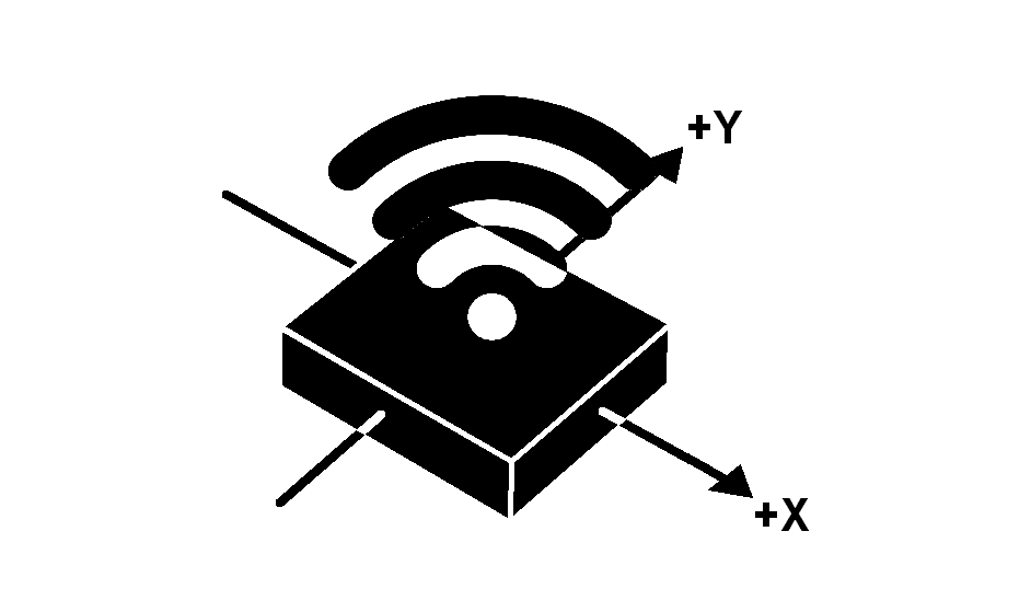
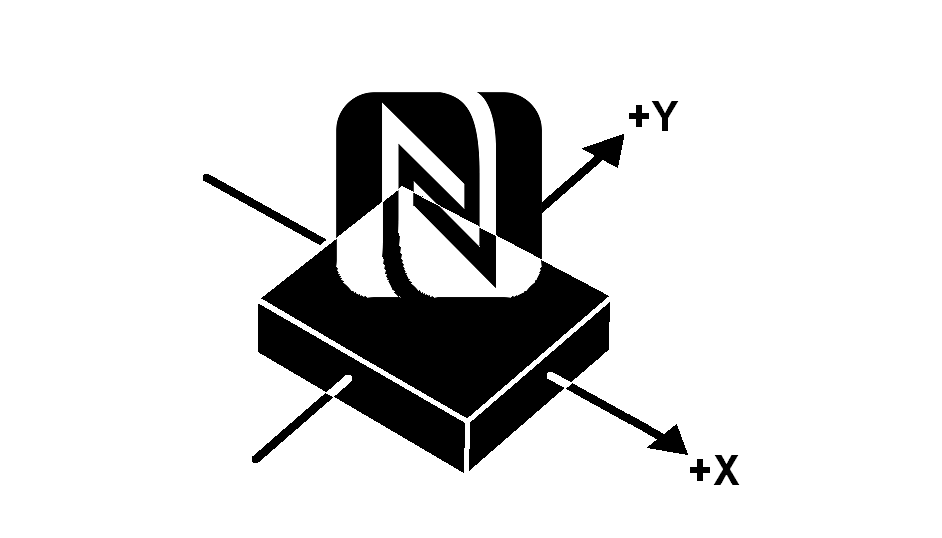
NFC
Non-technical Introduction
Although NFC is technically a wireless communication protocol, it is unlike all the other wireless communication protocols. Their are several NFC technical/non-technical quirks and features that make NFC stand out from all the other wireless communication prsotocols. For starters, in NFC the receiver is powered by the transmitter. Anther quirks that sets NFC apart from other wireless communication protocols is that neither the transmitter not the receiver have a “traditional” antenna and hence does not use radio waves for communication. Thirdly, unlike other wireless technologies which work though radio wave transmission, NFC works with inductive coupling. Finally, many times NFC has a reading/writing distance that is worse than wired cabling.
Technical Introduction
Inductive Coupling - At first glance, NFC more in common with a power transformer that a wireless transciever. Like a transformer, NFC works on the principle of inductive coupling. Unlike a transformer, NFCs core is air instead or iron core typically found in a transformer. This makes NFC exponentially less efficient than transformers. Furthermore, unlike a transformer which only transfers power, in a NFC setup data is also transmitted and received.
“Antenna” - Although NFC does contain an “antenna”, it does not contain an antenna in the traditional sense. Unlike other wireless communication protocols which have “traditional” radio antenna, NFC contains an inductive antenna. Unlike traditional radio antennas which are designed to capture/transmit radio waves, a NFC antenna are designed to efficiently capture changes in magnetic field. A NFC atenna is actually just an inductor made out of PCB trace. When it comes to NFC antennas, the reading/writing distance is directly affected by the antenna size. The bigger an NFC antenna, the greater the reading/writing distances, the smaller the perimeter the lesser the distance.
Distance - Out of all the wireless communication technologies, NFC offers the shortest transmitting distance. Unlike other wireless communication technologies which have even a decent transmitting/receiving distance, NFCs offers the subpar transmitting/receiving distance of 10 cm. In fact, NFCs transmitting/receiving distance is so short that many times cabling technologies, such as USB, offer better communication distances. Many times a wireless communication technology is used free an embedded system from being tethered. This often times begs the question of why bother using NFC when teaching options such as USB offer greater advantages. As will be explained latter, there is a perfect reason why 10 cm is an excellent reading/writing distance.
Roles - Typically NFC based ICs are classified into two
Initiator – The communication takes place between an active "initiator" device and a passive/active target device. The initiator actively generates an RF field that can power a passive target.
Active – The communication takes place between an active "initiator" device and a passive/active target device.
Passive -
Target device - The target device can either active or passive. Active means it has its own power source whereas passive means it does not have a power source and relies on the power source of the active initiator.
Active
NFC card emulation - Enables NFC-enabled devices such as smartphones to act like smart cards, allowing users to perform transactions such as payment or ticketing.
NFC reader/writer - Enables NFC-enabled devices to read information stored on inexpensive NFC tags embedded in labels or smart posters.
NFC peer-to-peer - NFC peer-to-peer communication is possible, provided both devices are powered. Enables two NFC-enabled devices to communicate with each other to exchange information in an ad hoc fashion.
Passive - The initiator device provides a carrier field and the target device, acting as a transponder, communicates by modulating the incident field. In this mode, the target device may draw its operating power from the initiator-provided magnetic field. This enables NFC targets to take very simple form factors such as unpowered tags, stickers, key fobs, or cards.
Tags, - NFC tags contain data and are typically read-only, but may be writable. They can be custom-encoded by their manufacturers or use NFC Forum specifications. The tags can securely store personal data such as debit and credit card information, loyalty program data, PINs and networking contacts, among other information. The NFC Forum defines four types of tags that provide different communication speeds and capabilities in terms of configurability, memory, security, data retention and write endurance. Tags currently offer between 96 and 4,096 bytes of memory.
Stickers,
Key fobs
Cards
Comparison with other wireless technologies
Data Rate
Transmission Distance
Power Consumption
Frequency Band
Bluetooth
2.1 Mbit/s
10 m (33 ft)- 100 m (330 ft) Bluetooth 5.0: 40–400 m (100–1,000 ft)
4
2.402 GHz - 2.480 GHz
Bluetooth BLE
1 Mbit/s
10 m (33 ft)- 100 m (330 ft)
15 mA (read and transmit)
2.402 GHz - 2.480 GHz
Bluetooth 5.0
x
Bluetooth 5.0: 40–400 m (100–1,000 ft)
x
x
Wifi
7
8
4
4
NFC
106 - 424 kbit/s
Less than 10 cm
15 mA (read)
13.56 MHz
ZigBee
15
16
4
4
Applications
Contactless payment systems.
Electronic ticket smart cards.
Sharing small files such as contacts.
Bootstrapping fast connections to share larger media such as photos, videos, and other files.
Typical Schematic
ZigBee
Peripheral Explanation
ECG
ECG Introduction
An ECG signal is a bio signal which is inherently produced by a beating heart as electricity travels throughout its “electrical conduction system”. An ECG signal can only be produced by a living mammal and is used in conjunction with other bio-signals helps asses the physiological health status of a patient. More specifically however, an ECG alone can tell the physician the physiological health status of the patient’s heart. Cardiac abnormalities, including cardiac rhythm disturbances (such as atrial fibrillation and ventricular tachycardia), inadequate coronary artery blood flow (such as myocardial ischemia and myocardial infarction), and electrolyte disturbances (such as hypokalemia and hyperkalemia) can all be detected through a ECG signal.
Electrical engineers whom are barely introduced to ECG theory find it is unlike non-bio circuit design theories. Two different and very distinct fields (biology and electrical engineering) come together during ECG design theory. As a result ECG design theory requires a solid understanding not only from an electrical engineer’s perspective but also from a biological perspective . This makes ECG design theory somewhat challenging, confusing and intimidating to beginning engineers or even seasoned engineers whom have switched to ECG theory.
In order to fully and properly grasp the concept of ECG system design theory, it is necessary to not only understand ECG from both perspectives but also the concepts within those perspectives. Furthermore, it is necessary to understand not only how concepts within perspectives interact but also how both perspective interact. Biology, for instance, has basic concepts (heart - purpose, importance, function, etc), mid-level concepts (action potential, polarization, depolarization, gap junctions, pacemaker cells, myocytes, depolarization wave, electrical impulse) and advance concepts (bio-electricity, cations, anions, ionic current, gradient, diffusion, etc). Conversely, electrical engineering has hardware perspective (circuit design, instrumentation amplifier, differential amplifier, low pass filter, PCB, schematic, layout, etc), firmware perspective (algorithm, RTOS, peripherals, hardware accelerators, registers, etc) and finally software perspective (CPU architecture, Operating System, wireless transceiver protocol, database management, etc). Furthermore it is necessary to understand how how bio-electricity leads to muscle contraction, how bio-electricity is propagated through the conduction system, how bio-electricity differs from conventional electricity, how bio-electricity gets converted to electron current.
ECG Introduction - Biological Perspective
Organs - All mammals including us humans are composed of a variety of organs. Humans, for instance, are composed of 78 organs. Examples of organs include brain, heart, lungs, kidneys, liver, pancreas, etc. Each and every organ has its purpose. Kidney(s) organ, for example, remove waste from the blood, stomach organ digest food, intestine organ extract nutrients from the food, lung organ replenishes carbon monoxide with oxygen, etc. Although the body can survive without some organs (spleen, appendix, etc), some organs (heart, brain, circulatory system, etc) are vital for life. Each and every organ is composed of discrete units called cells. Liver organ, for example, is made up of liver cells, kidney organ is made up of kidney cells, brain organ is made up of brain cells, etc. Each and every cell within each organs not only requires nutrients, but also produces byproduct. One thing that all organs have in common that they need a constant supply of blood.
Blood - Among other things, blood carries the nutrients (glucose, proteins, oxygen, etc) needed by every cell within every organ. Furthermore, blood also carries the waste byproduct produced by every cell within every organ. Lack of blood for short period of time results not only in cell starvation but also in cell waste intoxication. Lack of blood for long period of time results in cell death, organ failure and eventual organ death. Most organs, however, although vital for life, can withstand blood deprivation for a short period of time without facing serious-permanent life threatening consequences. Most organs posses cell regeneration capability. Once normal blood flow is reestablished, dead cells are disposed, replacement cells are generated, and organ function returns to normal. Unfortunately, the same cannot be said for neither the heart nor the brain.
Heart and Brain - Unlike other organs neither the heart nor the brain can withstand prolong blood deprivation. Unlike other organs, neither the heart nor the brain possess cell regeneration capabilities. This means that once normal blood flow is reestablished, dead cells will neither be repaired nor replaced. This presents a serious problem as the brain controls every facet of a persons being (muscular movement, thought process, speech, memory, etc) and the heart provides the nutrient and waste disposal necessary for organ life. It can be said that the brain is the most important organ and the heart the second most important organ in the human body.
Hearts Role - The fact that every organ directly depends on the heart for survival, exemplifies its importance. It is the heart’s job to not only circulate blood throughout each and every organ so that each gets its fresh set of nutrients but also so that every organ has a place to place their byproduct. Furthermore it is the job of the heart to circulate the blood through the “special” organs (kidneys, lungs, etc) that not only remove the cell waste from the blood but also replenish (lungs, small intestines, etc) it with fresh set of nutrients. Should the heart fail to carry out its job even for a fraction of a minute will be detrimental not only to itself, but also every other organ, including the brain. The fact that the brain is: the most important organ in the body, needs a never ending supply of nourishment and does not posses cell-regenerative capabilities highlights not only the heart’s importance but also its purpose.
Hearts Importance - The fact that every organ directly depends on the heart for survival, exemplifies its importance. It is the heart’s job to not only circulate blood throughout each and every organ so that each gets its fresh set of nutrients but also so that every organ has a place to place their byproduct. Furthermore it is the job of the heart to circulate the blood through the “special” organs (kidneys, lungs, etc) that not only remove the cell waste from the blood but also replenish (lungs, small intestines, etc) it with fresh set of nutrients. Should the heart fail to carry out its job even for a fraction of a minute will be detrimental not only to itself, but also every other organ, including the brain. The fact that the brain is: the most important organ in the body, needs a never ending supply of nourishment and does not posses cell-regenerative capabilities highlights not only the heart’s importance but also its purpose.
Heart Cell Types
Basic Heart Cell Type – The human body contains three types of muscle cells (skeletal, smooth and cardiac cells). No matter the muscle cell type, all muscle cells exhibit muscle contraction phenomena whereby electrical stimulation in the form of action potential triggers muscle contraction. Cardio cells are the ones found in the heart and they are directly responsible for a heart’s beating and pumping action. Cardio cells, unlike skeletal muscles, are involuntary muscle cells which means a person does not determent when and how they contract. Cardio cells are actually composed of two types of cells: myocyte and the autorhythmic cells. Both myocyte and the autorhythmic cells are electrically linked to one another, by structures known as gap junctions which allow the action potential to pass from one cell to the next.
Cardiac Myocyte Cells - The first type of cardio cells found within a heart are myocyte cells. Myocyte cells are not only the most abundant type of cardio cells found within a heart, but they are also directly responsible for the hearts pumping action. Like all myocyte cells and unlike “normal” cells, cardio myocyte cells possess this unique capability in that they can compress or reduce their dimensions at will. What dictates to a myocyte cell when to contract is an action potential wave. Whenever a “cardiac action potential” wave reaches any myocyte cell within a chamber, the entire myocyte cells that chamber simultaneously contract, creating the squeezing/pumping effect. Myocyte cells unlike pacemaker cells, don’t generate the action potential but instead simply propagate it.
Cardiac Autorhythmic Cells – The second type of cardio muscles cells found within a heart are cardiac autorhythmic cells. Autorhythmic cells are indirectly responsible for the pumping action of a heart but are directly responsible for the heart rate. Autorhythmic cells control the myocyte cells and instead set the pace of contraction. Unlike myocyte cells, autorhythmic cells can and do generate “spontaneous” action potentials. Furthermore, autorhythmic cells can also propagate an action potential wave. A heart contains a total of three clump of autorhythmic cells: Sinoatrial node (SAN) cells, Atrioventricular node (AVN) cells and Purkinje fibers.
Sinoatrial node/(SA) Node - The SA node comprises of a group of pacemaker cells located on the wall of the right atrium and whose purpose is to generate the initial cardiac action potential. The SA node is considered the primary pacemaker because it not only initiates the first action potential, but also dictates the heart rate. Under normal circumstance, the other pacemaker nodes “simply” propagate the SA node action potential. On average, the SA node generates 80 action potential per minute.
Atrioventricular node/(AV) Node - The AV node is also a group of pacemaker cells located between the left atrium and the right ventricle and that can both propagate and generate an action potential. On average the AV node generates 40-60 action potentials per minute. Under normal circumstances, AV node simply propagates the SA node action potential and “cancels” its own generation of action potential. However, should the SA node fail to generate the primary action potential, then the AV node takes over.
Purkinje fibers - Like the SA and AV nodes, the Purkinje fibers can both propagate and generate an action potential. On average the Purkinje fibers can generate 30-40 action potentials per minute. Under normal circumstances, the Purkinje fibers, like the AV node, simply propagates the AV node action potential and “cancels” its own generation of action potential. However, should the AV node fail to generate/propagate an action potential, then the Purkinje fibers takes over. The action potential rate of Purkinje fibers is slowest of the pacemaker nodes.
Bio-electricity
Introduction - Like all living creatures, mammals not only generate electricity but also use this generated electricity in all sorts of ways. However, unlike “traditional” current flow (electron over a copper wire) which electrical engineers are accustom to, bio-electricity, as it is called, consist of ions flow across cell membrane. The heart uses ionic current for both communication (stimulus) but also for muscle contraction (action potential) purposes. As will be explained later, the heart achieves its pumping action through series of well coordinated involuntary discrete muscle contractions caused by the electrochemical bio-electric wave propagating through the “electrical conduction system of the heart”.
Membrane Potential – Membrane potential is a necessary attribute inherent to all living cells. A cell’s membrane serves multiple roles, one of which is isolating the ions (potassium, sodium, calcium, and chloride ions) from inside of the cell to the ions external from it. Embedded throughout the cell’s membrane are both ion pumps and ion channels. Ion pumps transport ions from an area of low concentration to an area of high concentration. The area of high ion concentration can be either external or internal to the cell and vice versa for low ion concentration. Because ion pump transport ions against gradient, they require energy. Conversely, ion channels simply allow ions to naturally diffuse to an area of low concentration. Furthermore, ion channels, unlike ion pumps, don’t require energy to function. From an electrical engineering’s perspective, ion pumps and ion channels can be though of as batteries and resistors. Cell membrane, ion channels and ion pumps are what gives rise to membrane potential. Typical membrane potential values range between –40 mV to –80 mV.
Action Potential - One cell - Action potential is a electrochemical event that takes place within an excitable cell and which results in a momentary change in the cells membrane potential. There are a variety of reasons why an excitable cell would alter their membrane potential. Cardiac myocyte cells do it for heart muscle contraction while cardiac autorhythmic cells do it for cardiac myocyte manipulation purpose. Although change in membrane potential in non-excitable cells can also occur, strictly speaking action potential is applicable only for excitable cells. The act of altering ones membrane potential is called action potential. The act of a cardiac cell altering its membrane potential, it is called, not surprisingly, cardiac action potential.
Technically speaking an action potential is a brief reversal of the voltage cell polarity. Action potential is split into different phases; resting potential, depolarization, early depolarization, plateau, and finally repolarization. Furthermore, their are also some in-between events (stimulus and threshold potential) that are crucial in successful execution of action potential. It is worth mentioning that not all cardiac cells exhibits all of the phases. Autorhythmic, for example, don’t have neither stimulus nor early depolarization nor plateau phase. As a direct result, each cardiac cell type has a different action potential waveform.
Phase 4 - Resting Potential - Resting potential is a trait exhibited by all cardiac cells. Resting potential is a phase that all cardiac excitable cells exhibit both before and after executing an action potential. As the name implies, during a resting potential phase the cell could be considered resting (neither contracting nor generating an action potential). Resting potential is also the voltage both exhibited and measured across an excitable cell’s membrane. All cardiac excitable cells go through a resting potential phase after executing an action potential. Not all cardiac excitable cells exhibit the same resting potential. Furthermore, some cardiac excitable cells have static resting potential while others have “dynamic”.
Myocyte - As can be imagined a cardiac myocyte cell isn’t contracting during resting potential phase. The voltage exhibited/measured during a myocyte resting potential phase is dependent on which cardiac myocyte cell is being measured. The heart contains a variety of cardiac cells each with a different resting potential. Cardiac ventricular myocyte, for example, have a resting potential voltage of –90 mV. During resting potential cardiac chambers enough time for the resting chamber to be refilled with blood.
Autorhythmic – Technically speaking, autorhythmic cells don’t have a resting potential phase. Instead autorhythmic cells substitute resting potential phase for pacemaker potential phase. Autorhythmic cells cannot experience a resting potential phase as they need to periodically, constantly and autonomously generate an action potential. This is accomplished during a pacemaker potential phase in which case the membrane potential steadily increases. During pacemaker potential phase the cells membrane potential steadily increase until it surpasses the threshold and causes the cells to experience a self inducing action potential. The pacemaker potential could be seen as the stimulus phase.
Stimulus – A stimulus is a “signal” that “wakes up” a cardiac excitable cell. More specifically the stimulus rises the membrane potential and in the process takes the cells out of resting potential state. How long the stimulus is provided is directly correlated to the membrane potential voltage; the longer stimulus is provided, the more positive the membrane potential voltage. In both cases the stimulus is provided so long as the membrane potential is below the threshold potential. Once the stimulus brings the membrane potential up to the threshold potential, not only will stimulated cells generate an action potential but also the stimulus will be temporarily disabled. Typically the source of the stimulus is external however it can also be internally. Furthermore, the stimulus can either linearly or exponentially increase the membrane potential voltage. Moreover, int both cases the stimulus is source as long as membrane potential is below the threshold potential.
Myocyte - In the case of myocyte cells the source of the stimulus comes from neighboring myocyte/autorhythmic cells whom have just completed executing an action potential. Furthermore, in the case of myocyte cells stimulus is a byproduct of the action potential of the neighboring myocyte/autorhythmic cells. The influx of stimulus causes the cell membrane potential voltage to exponentially increase.
Myocyte stimulus consists of an influx of Na+ and Ca2+ ions across the cells membrane and into the cell cytoplasm. Each Na+ and Ca2+ ion carries a net +67 mV and +123 mV net charge. The influx of Na+ and Ca2+ ions will cause the membrane potential to jump from -90 mV to -70mv. The ions enter the cell through gap junctions (explained later).
Autorhythmic – Like a myocyte, the stimulus for autorhythmic cells can come from neighboring myocyte/autorhythmic cells. However unlike myocyte cells, autorhythmic cells can generate their own stimulus. When autorhythmic cells control their own stimulus, they control the membrane potential slope from resting potential to threshold potential. By controlling the stimulus, autorhythmic cells control the frequency between action potentials.
Autorhythmic stimulus consists of an influx of Na+ ions across the cells membrane and into the cell cytoplasm. Each Na+ ion carries a net +67 mV charge. The influx of Na+ ions will cause the membrane potential to jump from -60 mV to -40mv. The movement of Na+ ion is called “funny current”.
Threshold Potential - Threshold potential is another trait inherent to all cardiac cells. The addition of the stimulus to a cardiac cell does not continue forever. Eventually, the membrane potential equates to the threshold potential. Threshold potential is a constant numerical value which represents the voltage the membrane potential must reach. Once the membrane potential matches the threshold potential, the stimulus source stops sourcing its stimulus, and action potential process is triggered. Threshold potential varies by cardiac cell.
Myocyte - Myocytes cells have a -70 mV threshold voltage.
Autorhythmic – Autorhythmic cells have a -40 mV threshold voltage.
Phase 0 - Depolarization - Depolarization is another trait inherent to all cardiac cells. Furthermore, it should be emphasized that depolarization is the first step in action potential. Depolarization can best be describes as a cell’s internal reflex. Once the stimulus raises the membrane potential to the predefined threshold potential, depolarization takes over. As was discussed previously, every type of cardiac cell not only has a resting potential voltage but is has a different resting potential voltage (e.g., myocytes -90 mV and autorhythmic cells -40 mV). Anytime the cells membrane potential not only shifts from the resting potential but shifts in the positive direction (cell is less negative), a cell is being depolarized.
It should be emphasized that depolarize and depolarization is not the same thing. Although both stimulus and depolarization cause a cell’s membrane potential to depolarize, they accomplish it through different means. Depolarization, for instance, is self induced meaning that a cardiac cell own membrane potential causes itself to depolarize. In stark contrast stimulus uses ionic byproduct of neighboring cardiac cells to depolarize the membrane potential.
It is worth mentioning that the terms depolarize and depolarization are not the equivalent and should not be used interchangeably. Depolarize means whenever a cells membrane potential is shifted in the positive direction and in the process making the cell less negative. Furthermore, depolarize term can be applied to both stimulus and depolarization. Depolarization, however, is the act of a cell shifting its own membrane potential in the positive direction. Furthermore, depolarization term can only be applied whenever the membrane potential is above threshold potential.
Myocyte - Depolarization phase of myocyte cardiac cells is caused by the opening of fast voltage gated Na channels. This causes an influx of Na+ ions into the cells cytoplasm. Each Na+ ion carries a net +67 mV charge. The influx of Na+ ions will cause the membrane potential to jump from -70 mV to +20mv.
Autorhythmic – Depolarization phase of autorhythmic cardiac cells is caused by the opening of voltage gated Ca2+ channels. This causes an influx of Ca2+ ions into the cells cytoplasm. Each Ca2+ ion carries a net +123 mV charge. The influx of Ca2+ ions will cause the membrane potential to jump from -40 mV to +10mv.
Phase 1 - Early Repolarization - This is a phase that is applicable only to myocyte cells. The ionic current in this phase is caused by an efflux of K ions from the cell cytoplasm.
Phase 2 - Plateau - This phase is only applicable to myocyte cells. This phase is also known as plateau phase as it sits above the resting potential and is nearly flat. This nearly constant membrane potential is a direct result of equal number of Potassium ions (k+) entering the cell as the number of Calcium ions (Ca2+) exiting the cell. It is worth mentioning that muscle contraction not only occurs during this phase but is a direct result of this phase.
Phase 3 - Repolarization - Repolarization is another trait inherent to all cardiac cells. Furthermore, it should be emphasized that repolarization is the last step in action potential. Just like depolarization, repolarization can best be describes as a cell’s internal reflex. Repolarization is the opposite of depolarization; cell membrane potential is shifted back to the negative direction and in the process becomes more negative.
Myocyte - Repolarization phase of myocyte cardiac cells is caused by the opening of fast voltage gated K channels. This causes an efflux of K+ ions out of the cells cytoplasm. Each K+ ion carries a net -92 mV charge. The efflux of K+ ions will cause the membrane potential to jump from +5 mV to -90mv.
Autorhythmic – Repolarization phase of autorhythmic cardiac cells is caused by the opening of fast voltage gated K channels. This causes an efflux of K+ ions into the cells cytoplasm. Each K+ ion carries a net +123 mV charge. The influx of K+ ions will cause the membrane potential to jump from +10 mv to -60 mv.
Gap Junctions – One unique trait among cardio myocyte/autorhythmic cells is that they posses the capability to communicate with one another. The purpose of cardio cell-to-cell communication is to propagate the their action potential to neighboring cardio cells. This cell-to-cell communication is is achieved by way of gap junctions. Gap junctions are embedded throughout the entire cell membrane . Gap junction are hollow tubes which permit the passage/diffusion of ions from one cardiac cell to another. Although Na+, Ca2+ and K+. All myocyte/autorhythmic cells expel positive cations upon completion of their action potential. These cations can be considered the byproduct of the action potential.
ECG - Electrical Engineering Perspective
Introduction – Most engineers are surprised to discover that there is no such thing as a naturally occurring ECG signal. Instead it is a time-domain signal that is generated by a ECG circuit. Although an ECG signal is composed of action potentials, it is not itself an action potential measurement. Although action potential measurements provide enormousness heath status information, there is no non-intrusive and noninvasive known way of measuring it. The only known way of measuring an action potential is not only done in a lab settings, but requires extraction of the cardiac cell, penetrating its membrane with a probe, and finally measuring its potential difference across its membrane. Although action potentials cannot be directly measured, it can be indirectly measured by way of an ECG circuit. A ECG circuit is a non-intrusive analog based biomedical circuit that measures complex electrical activity of the heart, signal conditions it, and finally generates the now famous time-domain ECG analog signal.
Bio-signal reading – An ECG circuit measures the propagation of an action potential wave as it traverses the heart’s electrical conduction system. The ECG circuit works by observing the propagating action potential wave from two vantage points. Furthermore, as the ECG circuit is both concurrently and continuously sampling the wave as it is observing it. Moreover, each vantage point has a slightly different view of the propagation and hence generates a slightly different bio-signal. An ECG circuit exploits the fact that each vantage point generates a similar bio-signal but also that subtraction of these signals results in a signal which is indirectly proportional to action potential reading. One of the first problems that the ECG circuit must be overcome is how to convert the ionic current to traditional electron current.
Signal Conditioning - More often than not, the final destination of bio-signals produced by the electrodes is an ADC converter. However, the bio-signals obtained by the electrodes are not initially ready to be feed into the ADC. Although analog, the signals are not only too weak but also too noisy to be directly feed into the ADC. In essence the whole purpose of an ADC is to massage an ECG signal so that it is fit for insertion into an ADC. An ECG circuit is composed of discrete analog sub-circuits each of which is tasked at signal conditioning the signal so as to prepare the signal insertion into an ADC. As all bio-signals are inherently analog, the ECG circuit too is analog. Instrumentation amplifier, voltage amplifier, filter are just a few of the analog sub-circuits which comprise of the ECG circuit.
Introduction - Most if not all living creatures, including us mammals, use ion flow to generate electric current (cations and anions). This is unlike electric circuits which use electron flow to generate electric current. This presents a problem as ECG circuits only understand “traditional” electron carrying current. That is were electrodes comes in. Electrodes are electro-chemical sensors which are used to interface the ECG circuit with the patient. By definition, electrodes are a type of transducer. A transducer is any devices that lies in the boundaries of a “system” and converts one form of energy to another. In the case of an electrode, it is a (electrical) transducer and it lies between the patient’s skin and ECG circuit and it converts ionic current to/from traditional electron current. At most, the electrodes are able to conduct small currents. The electrodes are not directly adhered to the patients skin. Instead, sandwiched between the electrodes and the skin is an electrolyte gel whose purpose it to maintain good contact between the electrode and the skin.
Polarized vs non-polarized electrodes - There are two types of electrodes (polarized and non-polarized) and depending on the type of bio-signal that is being “analyzed” is the type of electrode that is used. Although ECG circuits, as will be explained, require non-polarized electrodes, it is worth discussing polarized electrodes as it gives the overall picture. What dictates whether the electrode is polarized or non-polarized is the type of metal used to construct it.
Polarized – Polarized electrodes are constructed out of Platinum (Pt). With polarized electrodes, direct current cannot cross the electrode-electrolyte-skin junction. Polarized electrodes are used for stimulation such as ___ and ___. Furthermore, polarized electrodes can/are modeled as capacitors.
Non-polarized - Non-polarized electrodes are constructed out of Silver/Silver-Chloride (Ag/AgCl). With non-polarized electrodes, direct current crosses the electrode-electrolyte-skin junction. Furthermore, non-polarized electrodes are modeled as resistors. Non-polarized are used for recording.
Ag/AgCl Electrode-Chemistry - As will be explained later, although there are a variety of electrodes available however the electrode of choice for ECG measurement is the Ag/AgCl electrode. What is meant by an Ag/AgCl electrode is that the electrode is made out of Silver however it has a thin coating of Silver-Chloride (AgCl) crystals. The purpose of the AgCl crystals is reduce noise in the electrode-electrolyte junction. A good question that should be asked is how exactly does an electrode convert electron carrying current (e-) into ion carrying current (Cl - and Ag+) when it enters a Ag/AgCl electrode. A lot of chemical reactions are taking place not only on the electrode-electrolyte junction but also at the electrolyte-skin junction.
Ag/AgCl Oxidation - When the current flows from the Ag/AgCl electrode to the skin, oxidation of the Ag electrode is the chemical reaction that is taking place. What this means is that individual Silver atoms withing the Silver electrode are loosing electrons and in the process becoming cations. These loose electrons are what is known as “convention” electron current. The loose electrons are sent down the copper wire towards the instrumentation amplifier. Conversely, the silver cation get immersed in the electrolyte gel and head towards the electrolyte-skin junction. As can be seen oxidation of the Silver electrode causes it to dissolve little by little.
Ag/AgCl Reduction - Conversely, when the current flows from the skin to the Ag/AgCl electrode, reduction of the Ag electrode is the chemical reaction that is taking place. What this means is that individual Silver cations floating in the electrolytic solution combine with the electrons coming from the copper wire and in the process becoming Silver atoms. The newly created Silver atoms adhere to the silver electrode. With reduction, electrons travel from the copper wires to the electrode. Conversely, the silver cation travel from the electrolyte-skin junction to the electrode. As can be seen reduction of the Silver electrode causes it to grow in mass.
Equivalent Circuit - As current travels through electrode-electrolyte and electrolyte-skin junctions, it encounters all sorts of impedance and resistance which not only affects current movement but also effects performance. Knowing not only what impedance and resistance are encountered but also knowing their values permits more accurate simulation of the ECG circuit. This not only helps gains insight, but also predicts performance and avoids costly mistakes. Fortunately, all it takes is a couple of resistors, capacitors and half cell potentials to simulate the impedance experienced by current as it travels through the electrode-electrolyte and electrolyte-skin junctions.
Half-Cell Potential - As discussed previously, the Silver cations that are immersed in the electrolyte gel have a net positive charge and the electrons that travel up the copper conductor have a net negative charge. Basic physics teaches us that equal polarities repel while opposite attract. At the electrode-electrolyte junction, the cations which are immersed in the electrolyte solution are attracted to the electrons on the copper trace. This phenomena is referred to as charge distribution (half-potential).
Electrode-Electrolyte junction - Even without the half potential distribution, the current must traverse two totally different mediums. Event though the oxidation-reduction chemical reaction is responsible for the passage of current, the conversion itself does create impedance. Fortunately, modeling this impedance is a straightforward process; a resister Rd in parallel with a capacitor Cd.
Electrolyte Gel Resistance - As can be surmised, ion current traveling through the electrolyte experiences much more impedance than electron current traveling through a copper conductor. Fortunately, modeling this electrolytic impedance can be accomplished with a straightforward resistor.
Electrolyte-skin junction - Similar conclusions can be reached for the electrolyte-skin junctions and skin impedance.
Hardware Perspective
The first order of business is the amplification of the signals obtained by the electrodes. Not only are weak signals susceptible to noise but they are also unfit for the ADC. The voltage range of a typical ECG signal lies in-between 1 mV ~ 5mV however the typical voltage range of most ADCs is 0 - 3.3 volts. This mismatch not only presents a problem but also results in an immense waste of ADC resolution resources. Basic mathematics dictates that 5mV is not even 1% of 3.3 volts. This means that if an ECG signal is directly feed into a ADC only uses 1% of an ADCs resolution will be used. By far the simplest solution is voltage amplification. By amplifying the ECG signal by a factor of 660, it is possible to get a full sweep of ADCs full resolution. Furthermore, amplifying an ECG signal makes it less susceptible to noise.
Inverting amplifier (IA) – Theoretically speaking we could run the two electrode signals through two voltage amplifiers to amplify them to levels more accommodating for ADC conversion. Furthermore, these theoretical amplifiers would have to be inverting as single-pole ADCs only understand positive voltages. Practically speaking however amplification with standard voltage amplifiers is simply not possible. Amplification, like all other measurement, is against a reference point. The easiest and most common, reference point electrical engineers use is ground or 0V. However in the analog world, the reference point neither has to be zero nor static. In the case of bio-potentials signals, they technically don’t have a reference point. Although the body can be grounded, that does not constitute a reference point.
The only known solution to this dilemma is to use a second electrode placed at a slightly different location and use that as a reference point. There is a reason why ECG circuits not only use two electrodes but why each are placed slightly apart. At any point int time each type of cardiac cell is in a different phase of action potential execution; some excitable cells might be in the beginning while other might be in the middle and still others are the ending stages. Add to this the fact that each cardiac cell has a different action potential waveform. Each electrode reading is a direct result of the contribution of every cardiac cell action potential. Any difference in reading is caused by both propagation delay and power dissipation caused by inverse-square law.
Differential amplifier (DA) – By simply adding an offset voltage to the non-inverting input of the IA, we create a somewhat different circuit. This new circuit is called a differential amplifier (DA). Unlike a IA which has one input, a DA has two inputs. Although a DA can be composed out of transistors, the one we will be focusing on is made of Operation Amplifiers. Most of the virtues of the IA has carries over to the DA. The DA, for instance, both amplifies and inverts the non-inverting input signal. A DA is a type of electronic amplifier that amplifies the difference between two input voltages but suppresses any voltage common to the two inputs. In order to get a good common-mode rejection ratio out of a DA it is vital that both R1 and R2 are equal. Symmetrical feedback network eliminates common-mode gain and common-mode bias.
Although in theory you could only use a DA to generate an ECG, in practice that is hardly if ever done. For all the virtues a DA has it also carries over the flaws from the IA. One of the fundamental rules towards measuring any system is you never disturb the system you are measuring. A DA has the potential to break that rule should the source not have a high impedance. This is due to in a DA neither of the inputs are directly feed neither into the amplifier inputs. Instead, the input form a voltage divider resistor circuit. A typical solution to this dilemma is by way of impedance matching.
Instrumentation Amplifier (InAmp) – It is possible to eliminate both impedance matching and source loading, both of which plague DA, simply by placing buffer amplifier (a.k.a - unity gain buffer, even voltage follower, or isolation amplifier) at the DA inputs. Buffer amplifiers isolate source signals from the DA input. Furthermore, the buffer amplifiers increase the input impedance of the circuit. Instead of traversing a resistor circuit and potentially changing its dynamics like it is done with a DA, the signals feed directly to the amp non-inverting inputs. All amplifiers by default have high input impedance (low bias current) and low output impedance which virtually eliminates the possibility of loading. The problem with this configuration is that the gain is static.
Buffer Amplifier (InAmp) – The overall amplification is increased by replacing the buffer amplifier with a non-inverting amplifier. In the analog world, amplification is almost never done in a single stage. In real life, analog amplification is typically done in multiple stages. Multistage amplification offer many advantages over single stage amplification; higher gain, less distortion, and improved frequency response are just a few of the advantages multistage amplifiers offer over single-stage amplifiers. ECG circuits also benefit from multistage amplification. In a ECG circuit, multistage amplification can be achieved simply by replacing the buffer amplifiers with non-inverting amplifiers. This can be done mainly because a buffer amplifier and non-inverting amplifiers are essentially the same circuits. A buffer amplifier is a non-inverting amplifier that has its R1 and Rf set to ∞ and 0, respectively.
Non-Inverting Amp – The two non-inverting amplifiers form the first stage and the differential amplifiers server as the second stage. Furthermore, first two non-inverting amplifiers are typically called the input stage and the differential amplifier is called the gain stage. Furthermore, this configuration shunts away negative feedback. Furthermore, this configuration increases the overall amplification of the circuit. This hypothetical circuit, although somewhat easy to understand specially for beginning engineers, is rarely if ever implemented in real life. Although a decent performance, a much more powerful circuit can be created simply by tying R1 together and in the process eliminating the ground connection.
Instrumentation Amplifier – The official name of this circuit is an instrumentation amplifier (InAmp). By tying resistor R1 together and eliminating ground we form an instrumentation amplifier (InAmp). In many instances the InAmp is considered the heart of the ECG circuit because its inputs also server and ECG circuit inputs and because the InAmp output can, although not recommend, be feed to the ADC. Additional characteristics include very low DC offset voltage, low drift, low noise, very high open-loop gain, very high common-mode rejection ratio, and very high input impedances. Moreover, and InAmp circuit can be constructed out of discrete OpAmps or it can be purchased single IC package. Both discrete based InAmps and IC based InAmps have their advantages and disadvantageous. That it even has a special name.
Low-pass filter
Noise – Although the output of the InAmp can be directly feed into the ADC, it would be immensely unwise to do so. As the action potentials traverses throughout the heart, muscles, skin, electrode, ECG circuit etc. they tend to “acquire” noise. As can be imagined, noise is both undesirable (distorts the measured signal) and inescapable (always present). Unfortunately, noise is most problematic in analog circuits as the whole analog signal has a significance. Technically speaking noise are random voltage fluctuation which get coupled to the signal desired to be measured. Thanks to Fourier Analysis we know that an ECG signal has a 0.5 Hz to 100 Hz frequency range with 0.02 mV to 5 mV amplitude. Any frequency component outside those ranges is noise and should be eliminated or at the very least mitigated. In an ECG circuit there are four main sources of noise and each sources of noise (EMG, baseline wondering, power line interference, and white Gaussian) has its amplitude and frequency.
EMG noise – The heart isn’t the only organ that generates action potentials. Turns out skeletal muscle, like cardiac cells, generate their action potentials only that they use for motor movement. ECG action potentials traverse the muscle tissue before reaching the ECG circuit. As the cardiac action potentials traverse the muscular tissue, the muscle action potentials generated by the tissue gets coupled to the ECG signal. During a EMG reading, EMG signals are the signal desired to be measured however during a ECG reading, they are considered noise. EMC signal has a 0 Hz to 500 Hz frequency range with 1 mV to 10 mV amplitude. Unfortunately, some of the signals are overlapped cannot be filtered frequencies non-overlapping frequencies are attenuated by the band-pass filter. Furthermore, EMC noise can be drastically mitigated simply by having relaxing the skeletal muscles during reading.
Baseline Wander – Another type of noise present in ECG signals is baseline wander. Baseline wander is generated at the electrode-skin interface and causes the ECG signal to drift either up or down in the spatial coordinate plane. More specifically, baseline wander is caused by improper electrode placement, patient motion, and/or respiration. Furthermore, baseline wonder can increase during strenuous exercise. Baseline Wander has a 0.5 Hz to 0.6 Hz frequency range with 0 V to 1 V amplitude.
Power line Interference – Electromagnetic induction is a phenomena which can be experience by any closed loop conductor. Electromagnetic induction dictates that a change in magnetic field induces an electric current in an enclose electrical conductor. In the case of a ECG circuit, the electrode cables form the conductor in a close loop and the dueling power lines generate a 60 Hz variable magnetic field. Although always present, PLC apparent itself on weak signals. One big problem with PLI noise is that its frequencies range (50 - 60 Hz) precisely overlaps ECG frequency range (0.5 - 80 Hz). A simple yet effective approach towards decreasing PLI is reducing the electrode loop size.
Analog Filter – Typically the ultimate destination of the ECG signal produced by the circuit a CPU. This presents a problem as CPUs only understand 1s and 0x. To remedy this, a ADC is used. As the name implies the ADC converts the time varying analog signal into its digital equivalent. CPUs are electronic devices that think, act, talk and behave in a “digital” manner; In fact the native language of a CPU is 0s and 1s. 0 represents 0 volts and 1 typically represents 3.3 and 5 volts. The output of the ECG is a time varying analog signal. This presents a problem as CPUs only understand in 1s and 0s. This is where the analog-to-digital (ADC) converter comes in. A ADC converts the analog signal to something the CPU can understand which is 0s and 1s.The job of the ADC is to break up the voltage signal into discrete units each representing the voltage/amplitude at that particular point in time. Like most things in life, there isn’t a one size fits all ADC architecture. Instead there are a variety of ADC architectures which can implement a ADC. Each architecture has its advantages and disadvantages. There are a variety of architectures to choose from (direct-conversion, successive approximation, ramp-compare, Integrating, Delta-Encoded, Pipelined, Sigma-Delta, Time-Interleaved, Intermediate FM stage, etc). Typical, it is a trade off is between sampling rate, power consumption and resolution.
Analog-to-digital
ADC – Typically, the ultimate destination of the ECG signal generated by an ECG circuit is the CPU. This presents a problem as CPUs are electronic devices that think, act, talk and behave in a “digital” manner; they only understand 1s and 0s. This is where the analog-to-digital (ADC) converter comes in. As the name implies the ADC converts the time varying analog signal into its digital equivalent. Like most things in life, there isn’t a one size fits all ADC architecture. Instead, there are a variety of ADC architectures which can implement a ADC. Typically it is a trade off between sampling rate and resolution. Since even the highest frequency component (aka bandwidth) in a ECG signal (~80Hz) is far lesser than even the slowest ADC, any ADC will technically suffice in ECG application. However, ΔΣ are typically used for ECG conversion due to their low cost and excellent resolution.
Electrodes vs. Leads
Single InAmp – It is possible to read/view the electrical activity of the heart with just one InAmp. By no means is this a ECG circuit as it is not only incomplete but also lacks many essential features (current protection, power supply isolation, etc) needed for consumer grade classification let alone medical grade classification. However, a one InAmp circuit does show the basic principles and theories (electrode placement, lead signals, lead vs electrode, etc) needed for mastering ECG circuit design. In fact most engineering students learn ECG circuit design theory by constructing these single InAmp bio circuit. All that is needed to construct this hypothetical ECG circuit is the InAmp, two electrodes, and an oscilloscope. The electrodes would be adhered torso at a locations which diagonally cross the heart. Furthermore, the output from the electrodes would serve as the input to the InAmp. Finally, the In InAmp output would be connected to the to the oscilloscope probe inputs. With this setup, the electrical activity of the heart would be measured. Of course this is only a theoretical setup as the oscilloscope are not only big, heavy, and bulky, but also extremely expensive.
Single InAmp Relocation – Convention dictates that a single InAmp does not constitute a ECG circuit. Although one InAmp has the capability to record the electrical activity of the heart, it can only do so from one “angle”. Although a great start, a straightforward/drastic improvement would be to record the electrical activity from multiple “angles”. Luckily this can easily be accomplished by physically moving the electrodes to a different position. Theoretically speaking this approach is the most economical one. However the disadvantage is that it requires physically relocating the probes and thereby causing discontinuity in readout. View requires one InAmp and two electrodes.
Limb Leads – Although relocating the probes is “A” solution, it is not the best solution. Relocating the probe during mid testing cause discontinuity in the readout. A better approach would be to incorporate multiple InAmps to the circuit. Incorporating multiple InAmps not only enables the reading of electrical activity from multiple “angles” but it does so concurrently and continuously. The obvious advantages to this setup is that it omits the probe relocation and it permits continuous multi-angle readouts. Nowadays silicone technology has progressed to such a point that it cost almost just much money fabricate one InAmp as it does to incorporate multiple InAmps. The electrode locations and their associated InAmp are refereed to as Limb Leads.
Augmented Limb Leads – There is an ingenuousness technique of creating three additional viewing angles without the need for additional electrodes. This technique only requires three additional InAmps, uses the exact same electrodes as those used by the Limb Leads, and does not require relocation of electrodes. Like previous defined techniques, one of the electrodes is directly connected to an InAmp input while the second electrode is indirectly connected to the InAmp. creates a virtual electrode by placonly one of the electrodes is directly connected to the InAmp while the other electrode(s) are indirectly connected tot he InAmp inputs.
Electrodes – In ECG terminology an electrode refers to the transducer-shielded cable-location combo that not only adheres to a patients skin and converts the ionic current produce by the patient into “traditional” electron current but also servers as input to the ECG circuit. Standardization dictates 10 electrodes should be used. Furthermore, not only does each electrode have a name, but has a predefined location which it must be adhered to. Typically, electrodes are grouped together and are collectively have a group name. Electrodes RA, LA, LL and RL referred to as limb electrodes. Limb electrodes are used to generate both Limb Leads and Augmented Limb Leads signals. Moreover, limb electrodes can be placed either in the limb extremities or on the torso area. A similar argument could be said of the remaining V1, V2, V3, V4, V5 and V6 electrodes which are collectively referred to as precordial electrodes. An electrode is not the same thing as a lead.
RA – On the right arm, avoiding thick muscle.
LA - In the same location where RA was placed, but on the left arm.
RL - On the right leg, lower end of inner aspect of calf muscle. (Avoid bony prominences)
LL - In the same location where RL was placed, but on the left leg.
V1 - In the fourth intercostal space (between ribs 4 and 5) just to the right of the sternum (breastbone)
V2 - In the fourth intercostal space (between ribs 4 and 5) just to the left of the sternum.
V3 - Between leads V2 and V4.
V4 - In the fifth intercostal space (between ribs 5 and 6) in the mid-clavicular line.
V5 - Horizontally even with V4, in the left anterior axillary line.
V6 - Horizontally even with V4 and V5 in the mid-axillary line.
Leads – Its tempting to say that the term Lead is the same as electrode. Furthermore, its also tempting to say that the term leads refers to the output of an InAmp. However, technically speaking Lead is a name given to InAmp output whose has certain electrode inputs. Sometimes the electrodes signals go directly to the InAmp inputs while in other times they pass through a circuit. Take for instance Lead I, which consists of the difference between the LA and RA. In this instance the electrode directly feeds the InAmp inputs. The same could be said for remaining Leads II and Leads III limb leads. For Augmented Limb Leads aVF, aVL and aVF it is a different story. Leads aVF is the name given to an InAmp output whose other intput is formed by the combination of LE and RL. In some instances the output of the electrode goes directly connected to the input of InAmps while in other time it goes indirectly connected. In other words sometimes electrodes are shared between InAmps (Limb leads vs Augmented Limb Leads).
Non-Inverting/Electrode(s)
Inverting/Electrode(s)
Lead Name
Right Arm
Left Arm
Lead I
Right Arm
Rigth Leg
Lead II
Right Leg
Left Arm
Lead III
Left Arm
Right Arm
Right Leg
aVF
Right Leg
Left Arm
Right Arm
aVL
Right Arm
Left Arm
Right Leg
aVR
V1
V1?
V2
V3
V4
V5
V6
V1 Septal
V2
V1
V2?
V3
V4
V5
V6
V2 Septal
V3
V1
V2
V3?
V4
V5
V6
V3 Anterior
V4
V1
V2
V3
V4?
V5
V6
V4 Anterior
V5
V1
V2
V3
V4
V5?
V6
V5 Lateral
V6
V1
V2
V3
V4
V5
V6?
V6 Lateral
Sorry
Congratulations!
You registration is officially complete.
Just register and start enrolling.
Sorry!
You registration has been rejected.
Congratulations!
Congratulations. Your registration has been
tentatively accepted. Please check your email
as a confirmation password has been sent you
you. Once you reply, you registration has
completed.
The title of the email is
Your registration with www.EmbeddedSystemSolution.com
Registration Error!
Sorry, server side errors were detected during
the registration process. Please read below to
see why you registration was rejected.
Registration form.
Log In
Log Out
Log Out
You have been successfully logged out.
We are so sad to see you leave. Please come back and visit us soon!
Congratulations!
Congratulations. You successfully logged into your
account. You can now register for training sessions,
request contractual services, make an appointment
with a specialist, access your custom dashboard,
apply for employment, etc.
Sorry!
Sorry, log in was unsuccessful.
Contact Us
Anonymous Question
(option A)
Be as descriptive as you want.
Block and Mortar Address
(option B)
Embedded System Solution
El Paso, Texas
79928
Phone
(option C)
Email
(option D)
Congratulations!
Anonymouse Question
Your anonymouse question has been
successfully submit and is
pending review. Please check
your email as we will most likely
respond there.
Thank you.
Embedded System Solution Team.
Sorry!
Anonymouse Question
Register first
Sorry you must register or log in prior to
Tech Support
Please select which better
describes what type of
Tech Support visitor you are.
Training Assistance
You are a visitor seeking training
assistance in Tech Support.
For those embedded system design
customers that are looking to
acquire the fine art of "host
side" app development, we offer
application development training
session assistance.
For those embedded system customers
that are looking to outsource their
"host side" application, we offer
contractual assistance were we built
a working prototype application.
For those customers that are in the
midst of a "host side" embedded application
and ran into a technical roadblock, we
also provide mid design consultation
assistance.
For those embedded system design customers
that are looking to aquire the fine art of
"taget side" PCBA design (Spice, schematic,
layout PCBA), we offer PCBA design trainning
services.
For those embedded system customers that
are looking to outsource their "target side"
PCBA design fabrication, we offer contractual
services were we built a prototype
system.
For those customers that are in the midst
of a embedded system "target side" PCBA design
and ran into a technical roadblock, we also
provide mid design consultation services.
For those embedded system design customers
that are looking to aquire the fine art of
"tagetside" firmware programing (SPI, I2C,
UART, USB, DMA, ADC, DMA, PWM, ARM, AVR,
MSP430) we offer firmware programing
trainning services.
For those embedded system design customers that
are looking to outsource their "target side"
firmware programming, we offer
contractual services were we both write
the firmware and provide the source code.
For those embedded system design customers that
are in the midst of writing their "target side"
firmware and ran into a technical roadblock, we
also provide consultation services were we answer
firmware related questions.
Before you can register to this
training session, you either have
to first log in or register.
Target Side Firmware experience
Most embedded systems nowadays
consist of a CPU (MCU, MPU DSP,
FPGA,) and a variety of sensor
ICs (WiFi, NFC, ECG, PPG,
Temperature) which give the PCB
target board capabilities. Furthermore,
variouse architectures.
CPU Architectural Experience
Although a PCB contains a variety of sensors, it contains just one CPU. The CPU is the part of the embedded system that makes decisions based on that data collected by the PCB sensors and external commands received from the user. There are a variety of architectures (MPU, MCU, DSP, GPU, FPGA) to choose from. Each architecture is built for a specific purpose and has its advantage and disadvantages. It is vital that CPU programmers know the differences when writing their application program and/or firmware. It is not the same thing writing a MPU application program as writing a MCU firmware application. Here at Embedded System Solution we have experience with the most popular CPU architectures.
MCU
MCUs are dedicated purpose
processors which means their
behavior and sense of purpose
is set in stone from the factory.
MCUs are low cost alternatives
to MPUs.
MPU
MPUs is a general purpose
processor which means its
behavior and sense of purpose
is not set in stone but
instead dictated by which
application is currently
executing.
DSP
DSP are specific purpose
processors that were invented
for the real-time processing
of continuously varying signals
(audio, image, etc )that make
up the real world.
GPU
GPU are specific purpose processors.
They are designed to render 3D objects
in real-time. Typical application include
3D gaming.
Standard on-chip Peripherals
Peripherals (a.k.a. hardware modules, hardware accelerators)
are tiny independent micro-circuits embedded in a CPU die that
give the CPU extra capabilities, reduces its power consumption
and/or increase its processing efficiency. Constructive use of
peripherals results not only reduction in embedded system power
consumption but also increases CPU instruction execution throughput.
Peripherals were invented/designed for off-loadable CPU tasks
(simple, mundane, repetitive, sequential and non-conditinal).
Whenever possible it is better to offload a off-loadable task
from the CPU to the peripherals as peripherals consume much less
energy than a CPU.
Timer
Timer peripheral generates a Timer Interrupt every x clock cycles. It can be sourced from either from CPU clock or external clock.
RTC
Real-Time Clock is a peripheral
keeps track of the current
time through the use of
an external 32.768 quartz
crystal.
WDT
WDT is a counter/timer like circuit that
resets the CPU. The WDT should be used
in situations where the firmware could
hang.
PWM
Pulse width modulation peripheral generates a configurable square wave with configurable frequency and duty cycle.
GPIO
Digital-to-analog
converter is a mixed signal
peripheral which takes an
CPU digital signal converts
it into its analog counterpart.
ADC
Analog-to-digital
converter is a mixed signal
peripheral which takes an
analog signal and converts
it into digital counterpart
for the CPU.
DAC
Digital-to-analog
converter is a mixed signal
peripheral which takes an
CPU digital signal converts
it into its analog counterpart.
Comparator
One of the most simplest
and basic peripherals, a
comparator compares the two
analog voltages and determines which
is the highest.
OpAmp
Pulse width modulation peripheral generates a configurable square wave with configurable frequency and duty cycle.
DMA
Direct memory access is an advance peripheral that handles peripheral-to-memory and memory-to-peripheral inform transfer.
LCD
Liquid Crystal Display is a hardware driver that handles the signals needed to drive a LCD.
USB
Timer peripheral generates a Timer Interrupt every x clock cycles. It can either from CPU clock, external clock or INT.
On-chip Serial Communication Peripherals for off-chip Peripherals
In many instances, its impossible to find the exact CPU-peripheral combo needed for your PCB project; either there is an excess (no problem) or absence (problem) of peripherals. Typically, the missing peripherals are either too specific or too complex. A typical solution is to use external discrete off-chip peripherals and use an on-chip serial communication peripheral. Common on-chip serial communication protocols include I2C, SPI, UART, CAN, etc.
I2C
CPU requires exactly two
pins (CLK and DATA) to
cummunicate with slave
devices. CPU can communicate
with up to 172 slave devices.
UART
CPU requires exactly two
pins (TX and RX) to
cumminicate with slave
device. The CPU can only
communicate with exactly
one device.
SPI
CPU requires only four pins
to cumminicate (MISO, MOSI, CLK & CS)
with initial slave device
and one additional pin for
each slave device after that.
CAN
CPU requires only two pins
to cumminicate (TX and RX)
with slave device however
it can communicate only
with one.
Off-Chip Wireless transceiver peripherals
Many times it is necessary for the PCB board to communicate with the outside word. There are a variety of wireless communication protocols technologies available. Typically, the PCB "target board" communicates with a "host side" computer application. Each protocol had its advantages and disadvantages. Typically the trade off is between power consumption and data throughput. Each communication protocol has it advantages and disadvantages.
Bluetooth
Bluetooth communication protocol
is a low power, short-range, mid
data througput wireless communication
protocol.
WiFi
WiFi communication protocol is a
high power, mid-range, mid data
throughput wireless communication
protocol.
NFC
NFC communication protocol is a
low power, short range, mid data
throughput wireless communication
protocol.
ZigBee
ZigBee communication protocol
is a mid power, mid range, mid
data throughput, wireless communication
protocol
Off-Chip MEMS peripherals
MEMS (micro-electromechanical system) are specialized integrated circuits packages which contain a conventional electrical circuit and a non-conventional mechanical system. The electrical circuit directly controls the mechanical side system. Furthermore, the mechanical system within a MEMS is created using the same semiconductor manufacturing techniques which is used to manufacturer electrical side circuit.
Accelerometer
Accelerometer is a class of MEMS IC which measures acceleration, typically, in all three axis. The acceleration can be static (gravity) or dynamic.
Gyroscopes
Gyroscope is a class of MEMS IC which measures angular velocity, typically, in three axis. The Gyroscope measures Roll, Pitch and Yaw.
Compass
Compass is a class of MEMS IC which is used to measure the earths magnetic poles. The compass measures west, east, north and south.
GPS
Not technically a MEMS IC however GPS technology is typically lumped together with MEMS ICs. Its provides precise geographical location.
Off-Chip environment peripherals
There are a varaety of environment
chips which measure the enviroment in
which they PCB board is
Temperature
Probably the most simple of the
enviroment peripherals, a temperature
IC measures the temperature where the
PCBA board.
Pressure
WiFi communication protocol is a
high power, mid-range, mid data
throughput wireless communication
protocol.
Humidity
NFC communication protocol is a
low power, short range, mid data
throughput wireless communication
protocol.
Barometer
ZigBee communication protocol
is a mid power, mid range, mid
data throughput, wireless communication
protocol
Off-Chip Bio-signal peripherals
Bio-signals are electrical-analog signals inherently produced by the human body and which can be used to help asses the physiological health status of the person. Bio-signal peripherals are electrical circuits that both measure and record bio-signals. Electrocardiography, photoplethysmography, electromyography, galvanic skin response, etc, are just some of the bio-signals generated by the body which can be both measured and recorded by bio-signal peripherals.
ECG
Electrocardiography (ECG) is bio-signal generated by the heart. The primary usage/application is to physician the physiological health status of the patient’s heart
PPG
Photoplethysmography (PPG) is a bio signal generated by the blood circulatory system. Its primary usage/application is to determine heart rate.
GSR
Galvanic skin response (GSR) is a bio-signal which measure the resistance of the skin. The resisitance is caused by perspiration of the skin.
EMG
ZigBee communication protocol
is a mid power, mid range, mid
data throughput, wireless communication
protocol
Product Software Assistance
Here at Embedded System Solution we
not only provide software assistance
for different types of software technologies,
but we also provide different types of
assistance. Whether the customer is looking
for training assistance, consultation
assistance or contractual assistance, we
can help.