Sorry

![]()
![]()
Please select which better describes what type of Tech Support visitor you are.

You are a visitor seeking training assistance in Tech Support.

You are a visitor seeking Tech Support contractual assistance.

You are a visitor seeking Tech Support consultation assistance.
For those embedded system design customers that are looking to acquire the fine art of "host side" app development, we offer application development training session assistance.
For those embedded system customers that are looking to outsource their "host side" application, we offer contractual assistance were we built a working prototype application.
For those customers that are in the midst of a "host side" embedded application and ran into a technical roadblock, we also provide mid design consultation assistance.
For those embedded system design customers that are looking to aquire the fine art of "taget side" PCBA design (Spice, schematic, layout PCBA), we offer PCBA design trainning services.
For those embedded system customers that are looking to outsource their "target side" PCBA design fabrication, we offer contractual services were we built a prototype system.
For those customers that are in the midst of a embedded system "target side" PCBA design and ran into a technical roadblock, we also provide mid design consultation services.
For those embedded system design customers that are looking to aquire the fine art of "tagetside" firmware programing (SPI, I2C, UART, USB, DMA, ADC, DMA, PWM, ARM, AVR, MSP430) we offer firmware programing trainning services.
For those embedded system design customers that are looking to outsource their "target side" firmware programming, we offer contractual services were we both write the firmware and provide the source code.
For those embedded system design customers that are in the midst of writing their "target side" firmware and ran into a technical roadblock, we also provide consultation services were we answer firmware related questions.
For our hardware customers needing target side PCB assistance (simulation, schematic, layout, PCB, etc), we provide a variety services (consultation, contractual and training) on a variety of hardware type boards (power, control, sensors, multi-layer, etc.). As can be seen, our PCB experience is not only wide but deep.
PCBA designing is unlike application development. For starters a software mistake is relatively inexpensive but also only takes seconds to repair. Hardware, on the other hand, is not only costly to repair but also takes orders of magnitude more time to repair. That is why PCB desigings simulater and re-simulate the PCB sub-circuit. Furthermore, many times PCB design not only requires mastery of electrical engineering concepts (ohms law, Kirchhoff’s current law, Kirchhoff’s voltage law, mesh analyses, superposition, etc) but also immense experience. It is not unheard of to hear that one engineer handles the conceiving section, while another engineer handles the schematic section, and while another handles the layout section.

We provide consultation assistance whereby during the initial conceiving phase we not only provide feedback (plausibility, power consumption, form factor, weight, plausibility, etc) on the proposed embedded system.
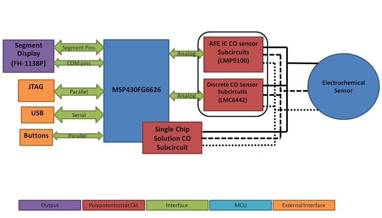
A block diagram is a high level view diagram image of the proposed embedded system. The block diagram contains blocks which represent all the major sub-circuit which compose the embedded system.
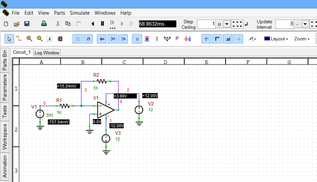
Prior to crating schematic/layout files, SPICE simulation should be done on the sub-circuits which compose the proposed embedded system. Simulation guarantees functionality, measure performance and saves money.
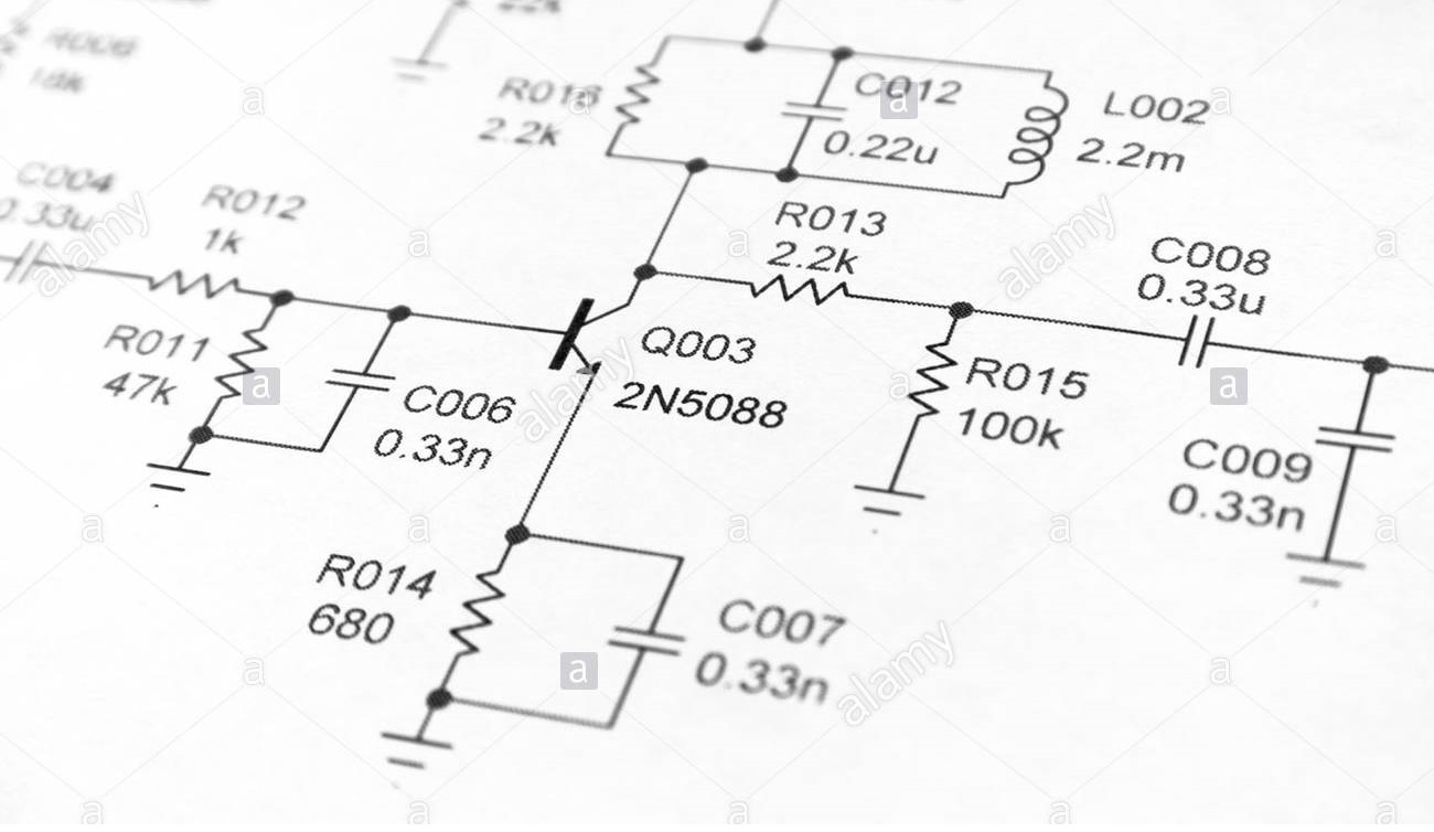
Schematics are the computer files which contain a graphical representation of the sub-circuits found on the PCBA. Comprehending/debugging a PCBA can be easily accomplished simply by glancing at the schematic files.
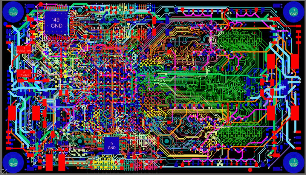
Layout is a computer file which dictates in exact detail the physical characteristics of the PCB. Board dimensions, board layers, electrical component placement, traces interconnect, etc. A layout file is created out of the schematic files.
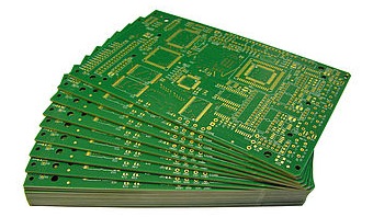
The Printed Circuit Board is the physical substrate which mechanically holds all the electrical components (resistor, capacitors, inductor, diodes, transistors and ICs) and the traces which interconnect these components.
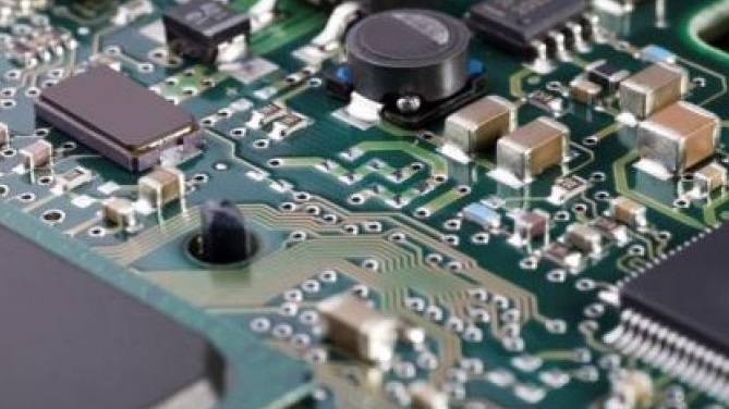
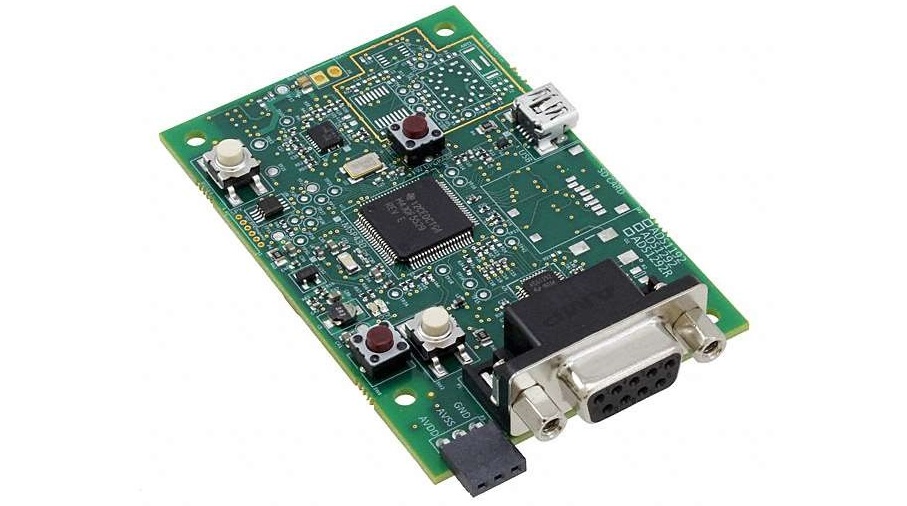
A printed circuit board assembly (PCBA) is a PCB populated with all the electrical components (resistor, capacitors, inductor, diodes, transistors and ICs). A PCBA is technically not an embedded system as it is lacking its enclosure.
ZigBee communication protocol is a mid power, mid range, mid data throughput, wireless communication protocol
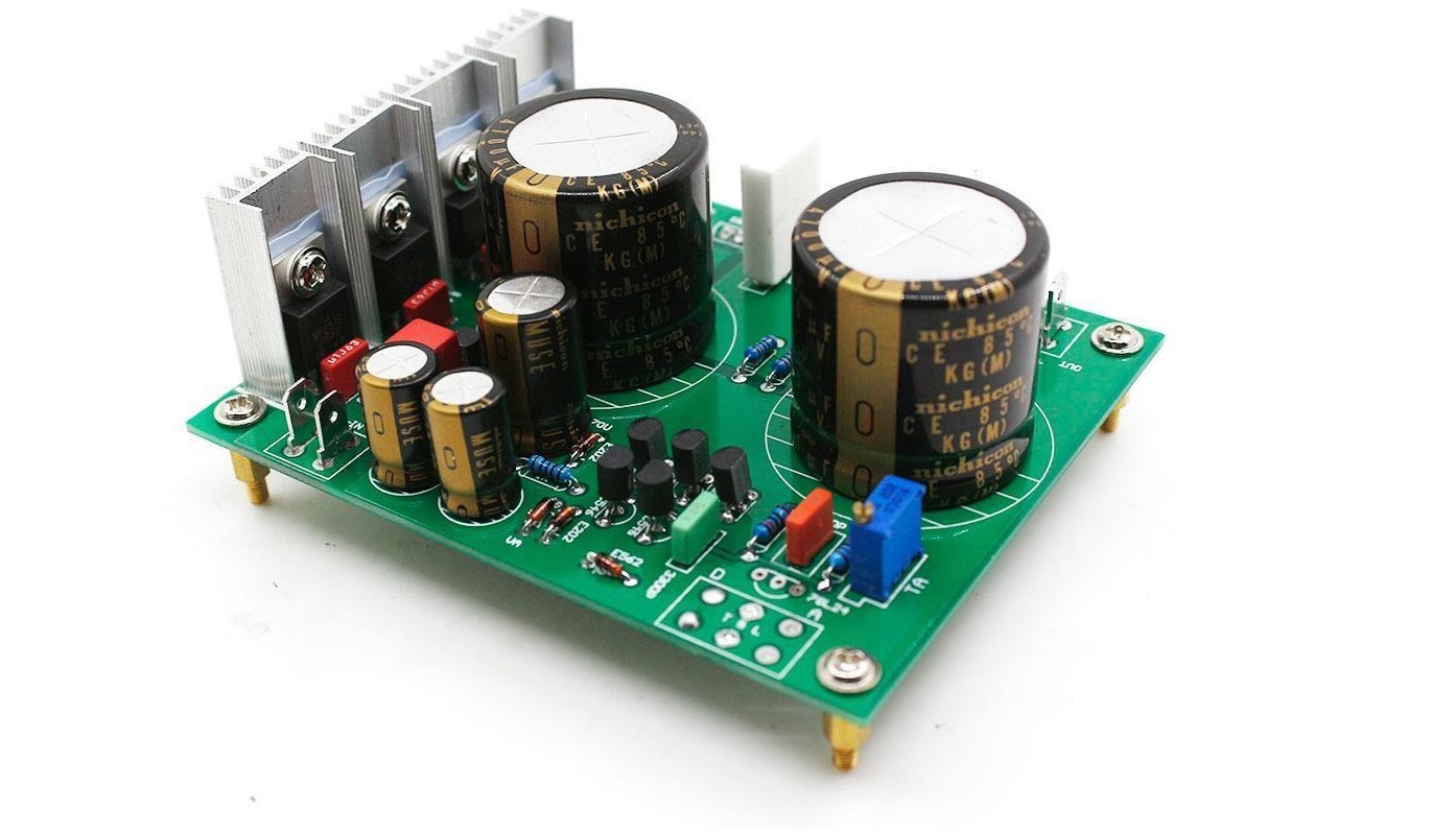
The following boards are examples of PCB boards which are purely hardware based and require no software.
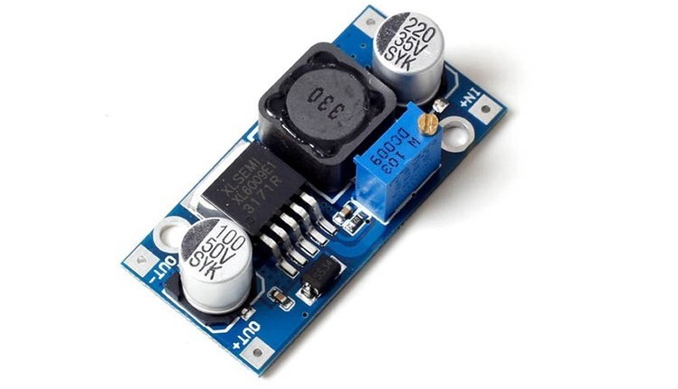
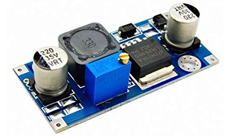
Type of DC-to-DC power converter which steps up voltage (while stepping down current) from its input (supply) to its output (load).
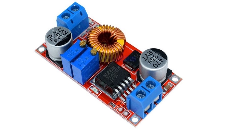
Type of DC-to-DC power converter which steps down voltage (while stepping up current) from its input (supply) to its output (load)
Charging circuit is responsible for recharging rechargeable batteries which if found on an embedded system.
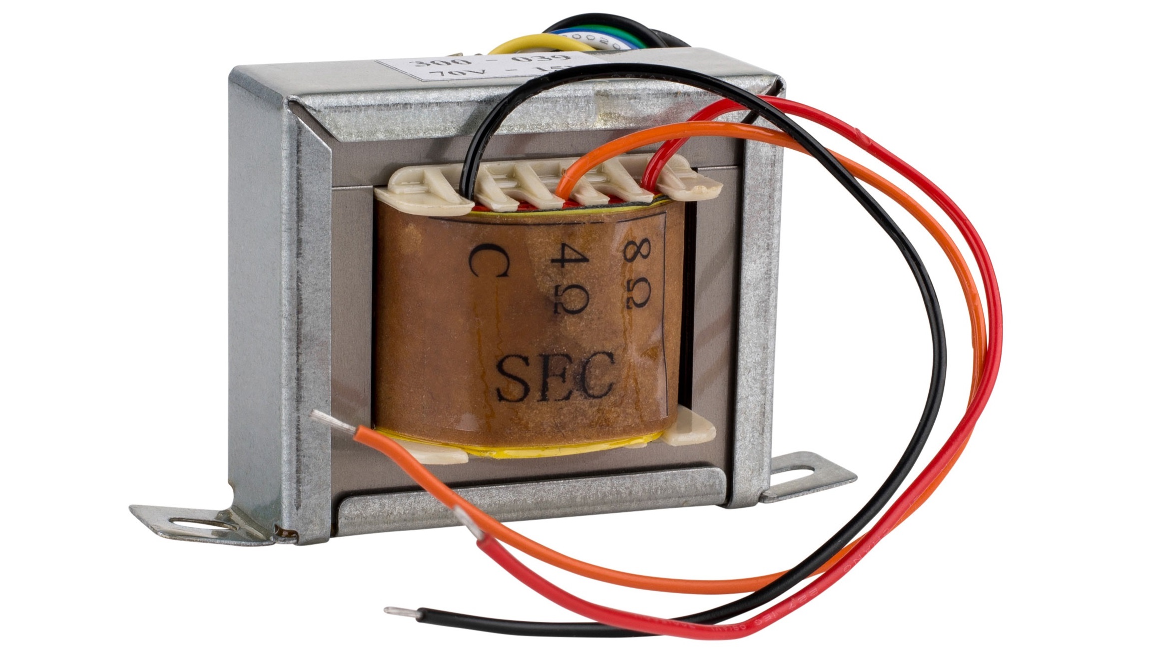
Electronic Power device which both regulates and/or converts the AC voltage. Typical input is 120 AC and 12, 6, 5, 3.3 DC and 50 AC output.
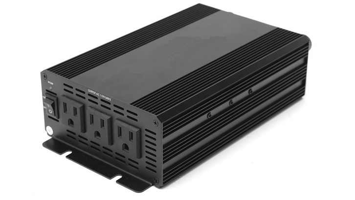
Electronic Power device which converts DC voltage to AC voltage (12 DC to 110 AC). Applications include cars and solar panels.
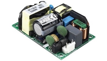
Electronic Power device which converts AC voltage to DC voltage (110 AC to 12 DC). Applications include everyday home appliances.
Electronic Power device which is used to either step-up (12 DC to 24 DC) or step-down (24 DC to 12 DC) a DC voltage.
Electronic Power device which either steps-up voltage (exp 110 AC to 220 AC) or steps-down voltage (exp 220 AC to 110 AC)
Here at Embedded System Solution LLC we have all the equipment necessary for both design and construction of a prototype embedded system. In-house PCB design equipment enables not only rapid and low cost prototyping, but also immediate turn around time. As can be expected, all of our equipment is the latest and greatest.
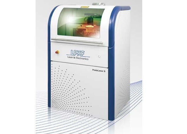
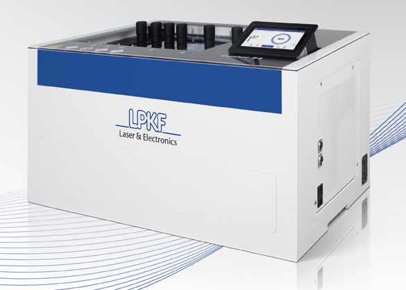
This PCB equipment which etches away the excess copper from a blank PCB and leaves only the traces and component pads.
This PCB equipment which adds a thin conductive layer of material to the walls of a via. This allows current to traverse the PCB.
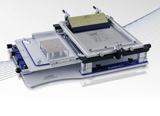
This PCB equipment which adds the solder paste to the PCB pads. It achieves this by using solder paste, stencil and a wiper.
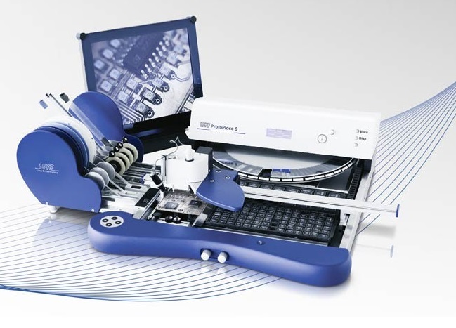
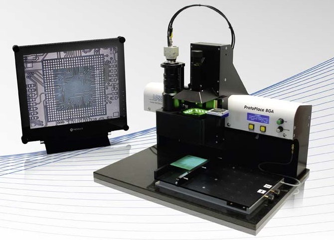
This equipment grabs the electrical components from a tape-and-reel and places them in their respective location on the PCB.
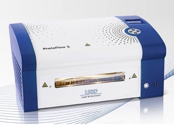
This PCB equipment melts the solder paste so that the legs of the electrical components can weld themselves to the PCB pads.
Bluetooth communication protocol is a low power, short-range, mid data througput wireless communication protocol.
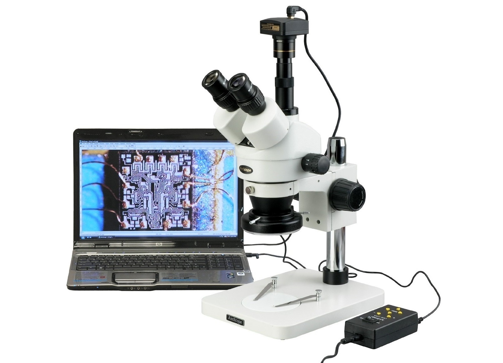
Stereo Microscope gives designers the capability to not only zoom in on PCB components but also add space between component and microscope lens.
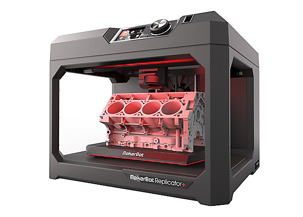
3D printers enabled designers to fabricate prototype enclosure for their embedded system thereby not only saving time but turnaround time.
